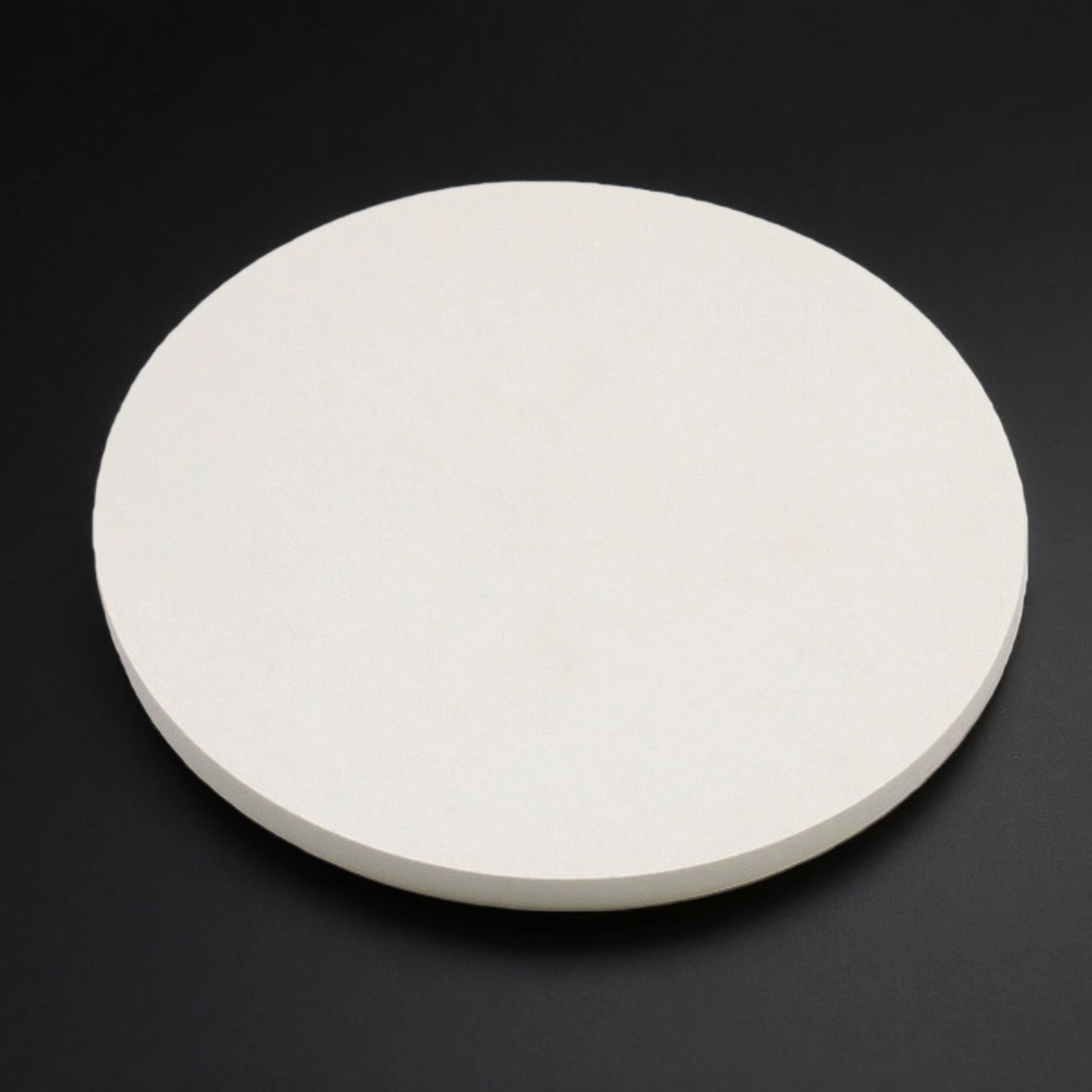
A Yttrium Oxide Sputtering Target is a dense ceramic body made from high-purity Y₂O₃, engineered to be mounted in RF or DC sputtering systems as the source material for depositing Yttrium Oxide thin films on substrates. During sputtering, energetic ions strike the Y₂O₃ target and eject atoms that form controlled dielectric or optical coatings, for example high-index layers in precision optics, high-k gate dielectrics, or functional films in photonics and R&D applications.
Yttrium Oxide Sputtering Target Benefits
-
High purity dielectric ceramic
Yttrium Oxide sputtering targets with 99.9–99.99% purity support low-defect dielectric and optical films, helping to control leakage current and optical absorption in the final coating. -
Dense microstructure for stable sputtering
Targets engineered toward the 5.01 g/cm³ theoretical density of Y₂O₃ reduce porosity and improve erosion uniformity, which supports consistent film thickness and composition across production runs. -
Controlled dielectric and optical performance
Y₂O₃ thin films can reach a dielectric constant around 14–18 and refractive index near 1.7–2.0, making the material suitable as a high-k dielectric and high-index optical layer in multi-layer stacks. -
Flexible target geometries for different cathodes
Yttrium Oxide sputtering targets can be made as discs, plates, column targets and step targets, matching round or rectangular cathodes on optical coaters, load-lock systems and R&D tools. -
Bonded and unbonded configurations
Y₂O₃ ceramics can be supplied unbonded for customer assembly, or indium-bonded to Cu or Mo backing plates to enable higher power densities and improved thermal control in RF or DC magnetron sputtering.
Yttrium Oxide Sputtering Target Properties
| Category | Property | Value |
| Chemical & Physical | Main Composition | 99% Y₂O₃ |
| Color | White | |
| Density | 4.9 g/cm³ | |
| Hardness (Mohs) | 6 | |
| Mechanical | Flexural Strength | 130 MPa |
| Compressive Strength | 508 MPa | |
| Thermal | Thermal Expansion Coefficient (25°C → 400°C) | 7.2 × 10⁻⁶ /°C |
| Long-Term Service Temperature | 800°C | |
| Thermal Conductivity (25°C) | 1.71 W/m·K | |
| Electrical | Dielectric Strength (5 mm) | 10 kV/mm |
| Volume Resistivity | > 10¹³ Ω·cm | |
| Dielectric Loss (25°C @ MHz) | Not specified | |
| Dielectric Constant (25°C @ MHz) | Not specified |
Yttrium Oxide Ceramic Sputtering Target Specifications
| Item No. | Diameter (mm) | Thickness (mm) | Purity |
| AT-Y2O3-BC01 | Customize | ||
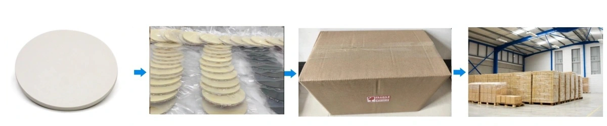
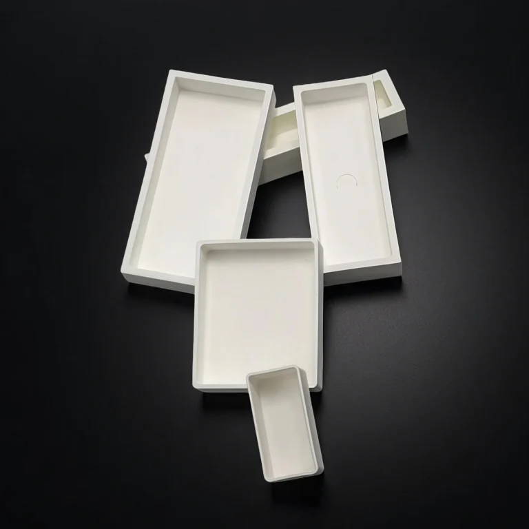
Yttrium Oxide Sputtering Target Packaging
- Each Y₂O₃ sputtering target is wrapped in clean, non-abrasive film and placed in a dedicated holder or cavity tray to minimize particle generation during transport.