High-Performance Silicon Nitride Ceramic Substrates for SiC & IGBT Modules
- Thermal-cycling toughness: high Si₃N₄ fracture toughness resists cracking and copper delamination (typical, application-dependent).
- Built for AMB/DBC modules: ceramic/copper thickness, pattern and outline made to your drawing.
- Review before quote: send a drawing or old substrate; we confirm feasibility and typical lead time.

80–100 W/m·K
Thermal Conductivity
(Stable Heat Dissipation for SiC / IGBT)
Resists Cracking Under Thermal Cycling
Compared to Al₂O₃ / AlN Substrates
What is a silicon nitride substrate?
A silicon nitride substrate is a high-performance Si3N4 ceramic plate used as the insulating, heat-spreading base under power electronic chips. After AMB or DBC metallization it carries the copper circuitry and SiC/IGBT dies, providing electrical insulation, heat dissipation and thermal-cycling durability in high-power-density modules. Actual performance depends on ceramic grade, thickness, copper design and your qualification.
Silicon Nitride Substrate Products
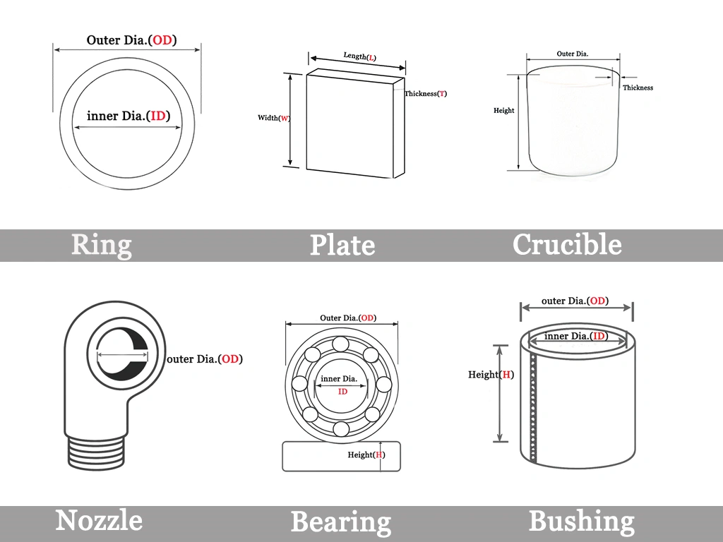
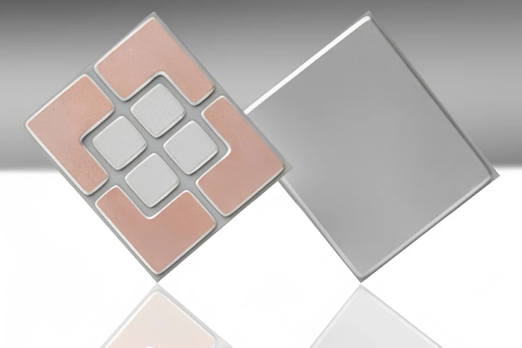
ADCERAX supplies silicon nitride substrates in multiple formats, including bare Si₃N₄ ceramic plates, AMB/DBC copper-metallized substrates, laser-cut custom shapes, and multilayer bonded designs.
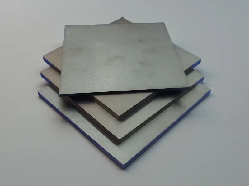
Silicon nitride substrates offer high bending strength and toughness, preventing cracks during soldering, pressing and thermal cycling in power module assembly.
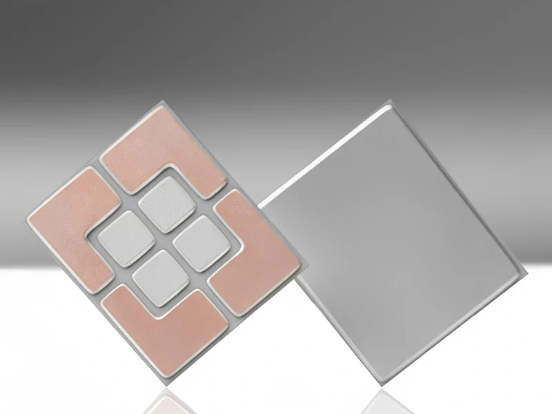
AMB silicon nitride substrates bond oxygen-free copper to Si₃N₄ ceramic using active metal brazing, creating a high-strength copper–ceramic circuit for power modules.
Why Si₃N₄ Substrates are Replacing Al₂O₃ and AlN in Power Modules?
Unlike alumina or aluminum nitride substrates, silicon nitride substrates provide better resistance to cracking and thermal stress, making it widely used in SiC and IGBT power modules.
| Parameter | Si₃N₄ (Silicon Nitride) | Al₂O₃ (Alumina) | AlN (Aluminum Nitride) |
|---|---|---|---|
| Thermal Conductivity | 80- 100 W/m·K | 20–30 W/m·K | 170–220 W/m·K |
| Fracture Toughness / Crack Resistance | ★★★★★ (High, resists cracking) | ★★☆☆☆ (Brittle) | ★★★☆☆ (Moderate) |
| Flexural Strength | ≥700 MPa | 300–400 MPa | 300–350 MPa |
| Thermal Expansion (CTE) | 2.8–3.2 ×10⁻⁶/K | 7–8 ×10⁻⁶/K | 4.5–5.3 ×10⁻⁶/K |
| Thermal Shock Resistance | Excellent | Poor | Moderate |
| Power Cycling Capability | High (Excellent resistance to cracking and delamination during repeated thermal cycling) | Low | Moderate |
| Typical Applications | SiC/IGBT power modules, EV inverters, wind & solar converters, industrial drives | Low-cost electronics, LED substrates, resistors | High thermal conductivity circuits, RF devices, heat spreaders |
Note: Power cycling performance is application-dependent. Actual cycles-to-failure vary with ceramic thickness, copper thickness, circuit pattern, bonding structure and test conditions. Final suitability should be confirmed through engineering review rather than assumed from a fixed cycle count.
Silicon Nitride (Si3N4) Substrate Properties
Si₃N₄ pairs heat-spreading thermal conductivity with high toughness for thermal cycling, low CTE for stress matching to Si/SiC and copper, and strong dielectric insulation. Ranges below are public typical values, confirmed per part on engineering review.
| Property | Unit / Condition | AD-SIN-SUB80 |
|---|---|---|
| Thermal Conductivity | W/(m·K); at 25 °C | ≥80 |
| Flexural Strength | MPa; material-selection value | ≥700 |
| Fracture Toughness | MPa·m½; method-dependent | ≥6.5 |
| Bulk Density | g/cm³ | ≥3.2 |
| Young’s Modulus | GPa; typical | 300–310 |
| Relative Permittivity, εr | At 1 MHz; typical | 8–9 |
| Dissipation Factor, tan δ | At 1 MHz; typical | 0.001 |
| Volume Resistivity | Ω·cm; at 20 °C | >10¹⁴ |
Advantages of silicon nitride substrates
High fracture toughness and flexural strength for thermal-cycling durability.
Thermal conductivity for heat spreading in high-power-density modules.
Low CTE for stress matching with Si/SiC dies and copper.
High dielectric strength and resistivity for insulation.
Suited to AMB/DBC metallization for thick-copper power layouts.
Where silicon nitride substrates are used
Silicon nitride (Si₃N₄) substrates are used in power electronics, EV and industrial inverters, and PV converters where thermal-cycling reliability and mechanical strength matter most. Their toughness and flat, stable form make them suited to compact, high-density SiC and IGBT modules..
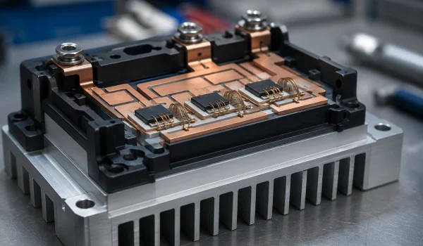
SiC / IGBT Power Modules
Application: Si₃N₄ substrates for SiC MOSFET and IGBT modules, DBC/AMB ceramic baseplates and power-cycling test boards.
- Why Si₃N₄ here:
- ~80–100 W/m·K with 600–800 MPa strength (typical) for high-power SiC/IGBT packaging.
- Low warpage (typical) for consistent solder layers and chip bonding.
- High fracture toughness resists cracking and copper delamination under thermal cycling.
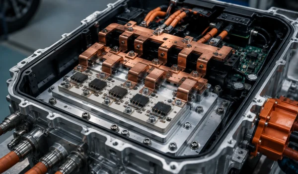
EV Power Inverters & OBC
Application: Si₃N₄ substrates for EV traction inverters, SiC drive modules, on-board chargers (OBC) and DC/DC converters.
- Why Si₃N₄ here:
- High toughness and copper adhesion (typical) withstand road vibration and thermal cycling.
- Low CTE for stress matching in compact, high-current SiC layouts.
- Suited to high-junction-temperature SiC module designs.
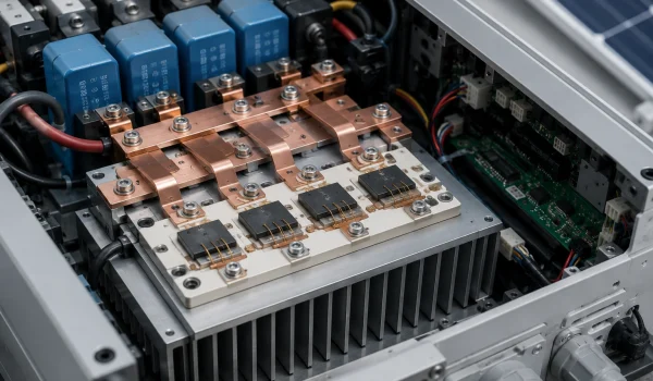
Solar Inverter Power Stage
Application: Si₃N₄ substrates for PV inverters, DC/AC conversion boards and grid-tied power modules.
- Why Si₃N₄ here:
- High dielectric strength (≥15 kV/mm, typical) for high-voltage DC stages.
- Strong thermal-shock and thermal-cycling durability (typical).
- Good copper adhesion for long-term outdoor reliability.
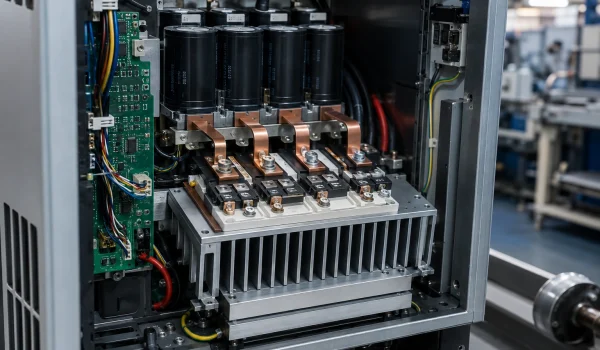
Industrial Inverter & Servo Drive
Application: Si₃N₄ substrates for VFD inverters, servo drive modules and motor-control power boards.
- Why Si₃N₄ here:
- 600–800 MPa strength (typical) resists cracking under vibration and torque stress.
- CTE ~3×10⁻⁶/K matches IGBT chips, reducing solder-joint fatigue.
- Low warpage (typical) for a stable thermal interface.
Silicon Nitride Substrates — Less Cracking, Less Delamination, Longer Power-Cycling Life
Si₃N₄ substrates reduce common module failures — cracking, delamination and solder fatigue — under repeated thermal cycling (typical, application-dependent). ADCERAX makes custom AMB/DBC substrates to your drawing, with engineering support for SiC and IGBT module manufacturing.
Custom Silicon Nitride Substrate Manufacturer
ADCERAX specializes in custom silicon nitride substrates manufactured according to your drawings or circuit layouts. We support non-standard thicknesses, complex shapes, laser-cut holes, surface metallization (AMB/DBC), multi-layer bonding, and copper circuit patterns for power module packaging. Both prototype samples and mass production are available with consistent quality and on-time delivery.
Customization Options
Extra-large / Extra-small diameters, non-standard thicknesses, and ultra-long / ultra-short lengths.
Provide higher - level dimensional accuracy and concentricity control than the standard.
Flanges, steps, threads, drilling holes, grooves, etc.
Adjust the material according to the application requirements.
Polish and grind the surface to achieve a specific surface roughness.
Customization Process
Send us your drawing, CAD file, or physical sample with material grade, dimensions, tolerances, and quantity. Our engineers will evaluate the design and provide a detailed quotation with lead time and pricing.
Once the quote is approved, we proceed with sample prototyping (1–50 pcs) if needed, for testing and validation.
After sample approval or direct confirmation, we begin batch manufacturing using CNC machining, sintering, and polishing. All parts undergo dimensional checks, material purity testing, and surface finish inspection.
Finished products are securely packed and shipped via DHL/FedEx/UPS or your preferred method. We support global delivery with full documentation.
ADCERAX — Silicon Nitride Substrate Manufacturing
ADCERAX runs the full Si₃N₄ substrate process in-house — forming, sintering, copper metallization (AMB/DBC) and precision machining, with inspection at each stage. From prototype to volume, this keeps flatness, copper adhesion and delivery under one roof.
Forming, sintering, AMB/DBC metallization and precision machining in one factory, for tighter quality control than an assembled supply chain.
Custom sizes, copper circuits, vias, stepped edges, multi-layer and laser-cut outlines from your Gerber, DXF or STEP files.
Low-warpage substrates and controlled surface finish for consistent solder layers and chip bonding in module assembly.
We check material, thickness, metallization and thermal-cycling fit before quotation, and support SiC/IGBT layout questions — with confirmed lead times by review.
| Manufacturing Capabilities Overview | |||
|---|---|---|---|
| Capability Item | Typical Value / Description | ||
| Material Grades | Hot-pressed / gas-pressure sintered Si₃N₄, high strength, fine-grain, optimized for AMB/DBC bonding and thermal cycling | ||
| Precision Machining | CNC grinding, laser cutting and ultrasonic drilling; tightest tolerances down to ±0.005 mm (thickness) and ±0.01 mm (dimensions), low warpage, and smooth surfaces for SiC/IGBT die bonding. | ||
| Forming & Shaping | Custom sizes, stepped edges, chamfers, vias, cavities and multi-layer laminations before metallization | ||
| Flatness & Microstructure Control | Controlled sintering atmosphere, fine Si₃N₄ powders (<1 µm), stress-relief grinding for density, low porosity and flatness | ||
| Copper Metallization (AMB /DBC) | Active Metal Brazing (AMB) and Direct Bonded Copper (DBC) for 0.2–0.8 mm copper; copper peel strength 16–29 N/mm (standard ≥10 N/mm), high thermal-cycling durability and customizable circuit patterns. | ||
FAQ about Silicon Nitride Substrates
Yes. SiC devices run at higher temperature and switching frequency. Si₃N₄ substrates provide strong insulation, good heat dissipation and high mechanical toughness, which supports reliability under high-temperature, high-current and repeated thermal cycling (typical, application-dependent).
We support AMB and DBC copper metallization, plus Ni/Au plating on request. Copper is 0.2–0.8 mm; common builds are 0.3/0.3 mm and 0.3/0.2 mm on 0.25–0.32 mm Si₃N₄. Thicker copper is available for high-current modules — confirmed by drawing review.
Standard ceramic thicknesses are 0.25, 0.32, 0.38, 0.5 and 0.63 mm; custom 0.2–2 mm. Maximum plate size is typically around 140 × 190 mm (custom on request).
Its high fracture toughness resists micro-cracks during soldering and thermal swings, reducing interface fatigue between copper, ceramic and chip. This gives significantly longer power-cycling life than alumina in typical testing.
Si₃N₄ offers the best toughness and thermal-cycling durability (thermal conductivity ~80–100 W/m·K, typical). AlN has higher thermal conductivity but lower mechanical strength; Al₂O₃ is the most economical but has the lowest thermal conductivity. Choose Si₃N₄ when power cycling, high voltage or reliability drives the design — send your operating conditions and we help confirm the fit.
Yes. We accept Gerber, DXF or STEP files for custom copper circuits, vias, cavities, stepped edges and double-layer copper–ceramic–copper builds.
Typical failures are ceramic cracking, delamination, solder voids and copper lift-off. Si₃N₄ reduces these risks through higher mechanical strength, low warpage and strong copper adhesion.
Send dimensions and thickness, format (bare / AMB / DBC), a drawing (PDF, DXF, Gerber or STEP), quantity and any special requirements to info@adcerax.com or WhatsApp. Our engineers reply with feasibility, pricing and typical lead time — usually within 24 hours.
What to Send for a Silicon Nitride (Si₃N₄) Substrate Quote
For a fast engineering review, please share:
- ceramic thickness (e.g. 0.25 / 0.32 / 0.635 mm)
- copper thickness and format — bare, AMB or DBC
- pattern / outline drawing — PDF, DXF, Gerber or STEP
- surface finish requirement (target Ra)
- working voltage and thermal-cycling target
- application (SiC/IGBT power module, EV/industrial inverter, PV converter)
plus quantity — prototype or production. Our engineers confirm feasibility, ceramic/copper thickness and typical lead time by review before quotation.
*Our team will answer your inquiries within 24 hours.
*Your information will be kept strictly confidential.
info@adcerax.com
Tel:+86-0731-84428843
WhatsApp:+86 19311583352
Within 24 hours