Alumina Ceramic Substrates (Al₂O₃): RF, LED & Electronic Circuit Substrates
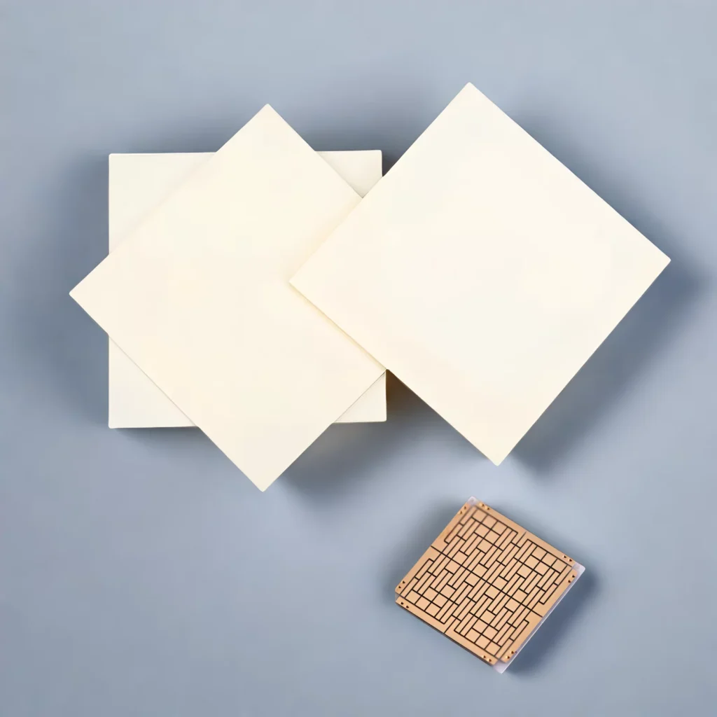
ADCERAX is a China-based direct manufacturer of alumina ceramic substrates (Al₂O₃) for electronics, RF, LED and laboratory applications. We supply 95%, 99%, 99.5% and 99.6%–99.7% purity grades, with polishing, laser drilling and metallization reviewed from your drawing — supporting prototypes through repeat production.
Standard sizes cover common thick-film and thin-film formats; custom sizes, holes, scribe lines and surface finishes are confirmed through engineering review before quotation. Products include blank substrates, metallized Al₂O₃ substrates, and thin- and thick-film circuit carriers — so your substrate matches the circuit process, not just the price.
1730°C
Max Operating Temp
(99.9% Purity)
Tight Thickness & Flatness Control (Polishing, Drilling, Metallization)
Factory Direct Supply
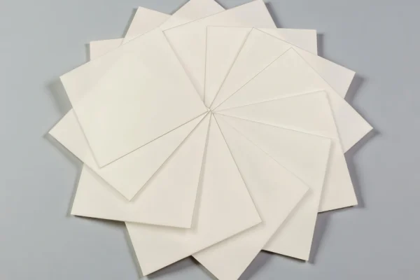
What is Alumina Substrate?
Alumina substrate is a ceramic sheet made from Al₂O₃, used as an electrical insulator and mechanical carrier in electronic circuits and high-temperature devices. With stable dielectric constant, moderate thermal conductivity, and excellent chemical resistance, alumina ceramic substrates are widely applied in RF packaging, LED modules, and laboratory fixtures.
Alumina Substrate Thickness and Spec
Choosing the right high alumina substrate thickness helps balance performance and cost. ADCERAX offers all thickness ranges with tight tolerance control, making it easy to move from prototypes to mass production.
Thin Substrates (0.3–0.5 mm)
- Application: High-frequency circuits, lightweight PCB designs, R&D samples
- Advantages: Reduced weight, suitable for microwave & RF use, easy for prototyping
Standard Substrates (1–2 mm)
- Application: PCB-like carriers, LED modules, thick-film circuits
- Advantages: Most versatile, balances strength and processability, widely stocked
Thick Substrates (≥3 mm)
- Application: Power modules, heat spreaders, structural carriers, precision fixtures
- Advantages: High mechanical stability, excellent heat dissipation, reliable for high-power devices
Common Alumina Substrate Sizes
Common formats we regularly produce. Availability and custom sizes are confirmed per RFQ.
| Size (mm) | Thickness | Purity | Surface | Stock Status |
|---|---|---|---|---|
| 25.4 × 25.4 (1″ sq) | 0.5 / 1.0 mm | 96%, 99% | Polished | ✅ Common size |
| 50.8 × 50.8 (2″ sq) | 0.5 / 1.0 / 2.0 mm | 96%, 99%, 99.7% | Polished | ✅ Common size |
| 100 × 100 | 0.5 / 1.0 / 2.0 mm | 96%, 99% | Polished | ✅Common size |
| 114 × 114 (4.5″ sq) | 0.635 / 1.0 mm | 96% | As-fired / Polished | ✅ Common size |
| 150 × 150 | 1.0 / 2.0 mm | 96% | As-fired | ✅ Common size |
| Ø50.8 (2″ round) | 0.5 / 1.0 mm | 99%, 99.7% | Polished | ✅ Common size |
Alumina(Al2O3) Ceramic Substrate Type
ADCERAX provides alumina ceramic substrates in 95%–99.7% purity with both standard sizes and custom machining options. From stock parts to special designs, we ensure stable quality and competitive pricing directly from our factory.
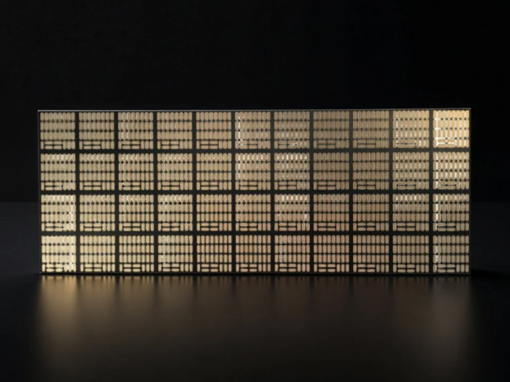
metalized alumina substrate
Metalized alumina substrates provide reliable low-resistance connections for power modules, LEDs, lasers, and sensors.
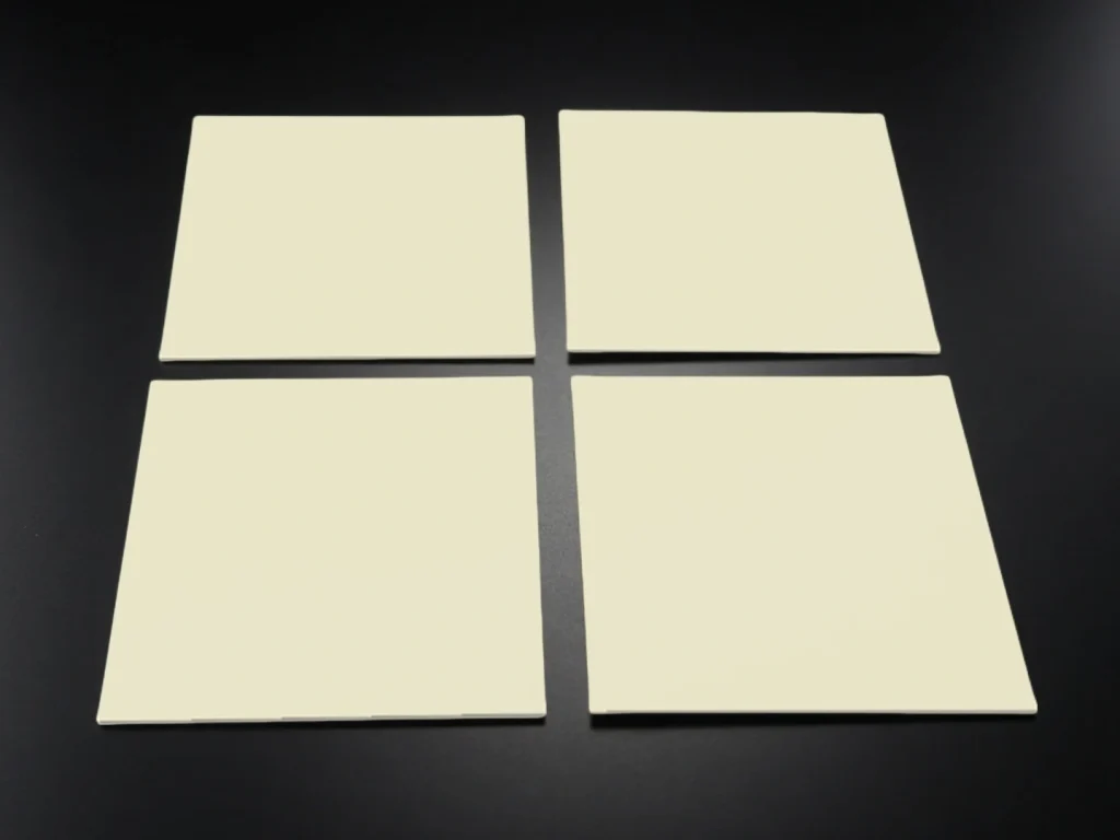
High Purity alumina substrate
High-purity alumina substrates (99.6%–99.7%+) offer insulation, flatness, and thermal stability for semiconductor and electronic applications.
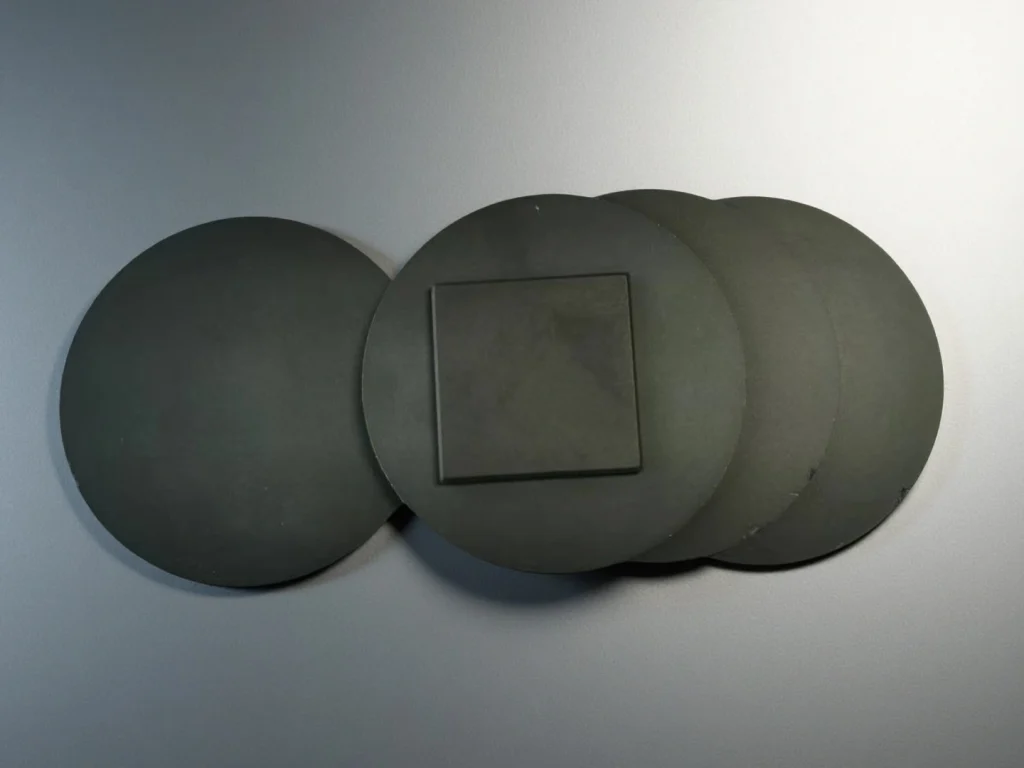
Black alumina ceramic substrate
Black alumina ceramic substrates combine strength and anti-reflective performance for optical, infrared, and electronic applications.
Alumina Substrate Properties & Benefits
🔌 High Dielectric Strength
Alumina sheet substrate provides stable insulation up to 15–22 kV/mm, ensuring reliable performance in RF circuits, LED packaging, and high-voltage power devices.
🌡️ Thermal Management
With thermal conductivity between 18–29 W/m·K, substrates enable efficient heat dissipation for LEDs, sensors, and microwave modules, extending device lifetime.
📏 Tight Tolerance Control
Precision flatness and thickness tolerance down to ±0.05 mm allow consistent circuit printing, laser drilling, and metallization, reducing defects in production.
⚙️ Versatile Processing Options
Available in thin (0.3–0.5 mm), standard (1–2 mm), and thick (≥3 mm) formats, alumina substrates support screen printing, sputtering, and custom metallized layers for diverse applications.
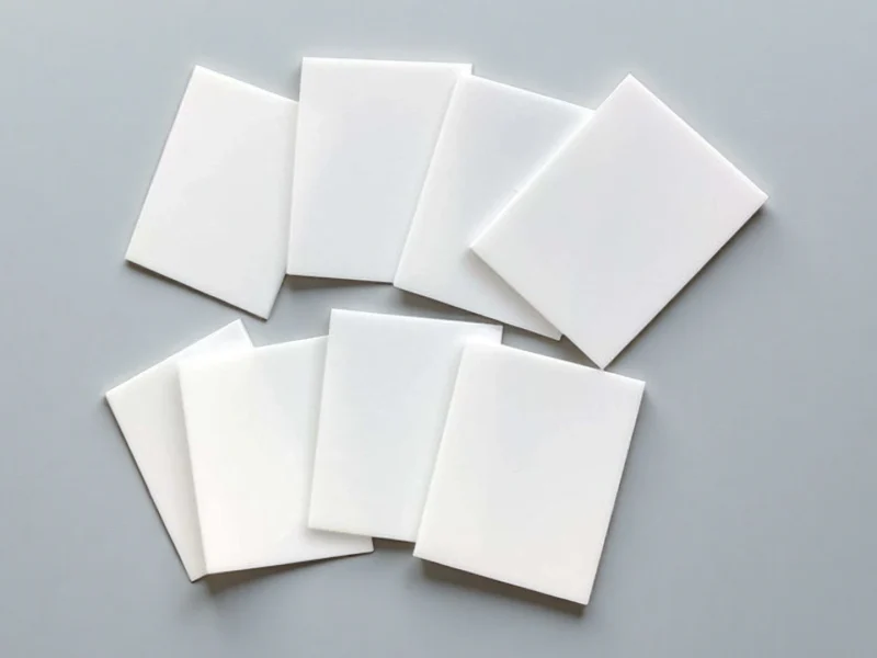
| Purity Level | Mechanical Properties | Thermal & Electrical Properties | Typical Applications | Key Advantages |
|---|---|---|---|---|
| 95% Al₂O₃ (C795) | Density: 3.75 g/cm³; | Long-Term Temperature: 1,400°C; Thermal Conductivity: 18–25 W/m·K;Dielectric Strength: 10 kV/mm; Volume Resistivity: >10¹² Ω·cm | General electronic substrates, hybrid circuits and insulating supports | Suitable for general-purpose substrate applications |
| 99% Al₂O₃ (C795) | Density: 3.80–3.91 g/cm³; Hardness: 9 Mohs; Flexural Strength: 300–320 MPa;Compressive Strength: 2,400 MPa | Long-Term Temperature: 1,600°C; Thermal Conductivity: 24 W/m·K; Dielectric Strength: 10 kV/mm; Volume Resistivity: >10¹⁴ Ω·cm | Electronic substrates, power modules and LED packages | Higher resistivity and temperature capability than the 95% grade |
| 99.5% Al₂O₃ (C799) | Density: 3.90–3.92 g/cm³; Hardness: 9 Mohs; Flexural Strength: 320–350 MPa;Compressive Strength: 2,400 MPa | Long-Term Temperature: 1,650°C; Thermal Conductivity: 30–38 W/m·K;Dielectric Strength: 10 kV/mm; Volume Resistivity: >10¹⁴ Ω·cm | High-reliability circuit substrates, RF devices and precision electronics | Higher thermal conductivity with tan δ <0.0001 at 1 MHz |
| 99.7% Al₂O₃ (C799) | Density: 3.94 g/cm³; Hardness: 9 Mohs; Flexural Strength: 330 MPa;Compressive Strength: 2,500 MPa | Long-Term Temperature: 1,700°C; Thermal Conductivity: 35–40W/m·K;Dielectric Strength: 10 kV/mm; Volume Resistivity: >10¹⁴ Ω·cm | RF and microwave substrates, sensors and high-performance electronics | High thermal conductivity, low dielectric loss and consistent material properties |
| 99.9% Al₂O₃ (C799) | Density: 3.94 g/cm³;Hardness: 9 Mohs;Flexural Strength: 315–340 MPa;Compressive Strength: 2,558–2,900 MPa | Long-Term Temperature: 1,750°C; Thermal Conductivity: 35–42W/m·K;Dielectric Strength: 10 kV/mm;Volume Resistivity: >10¹⁴ Ω·cm | High-purity circuit substrates, semiconductor packaging and RF/microwave electronics | Highest purity, high compressive strength and thermal conductivity, with tan δ <0.0001 at 1 MHz |
Polished Alumina Substrates: Surface Finish Options
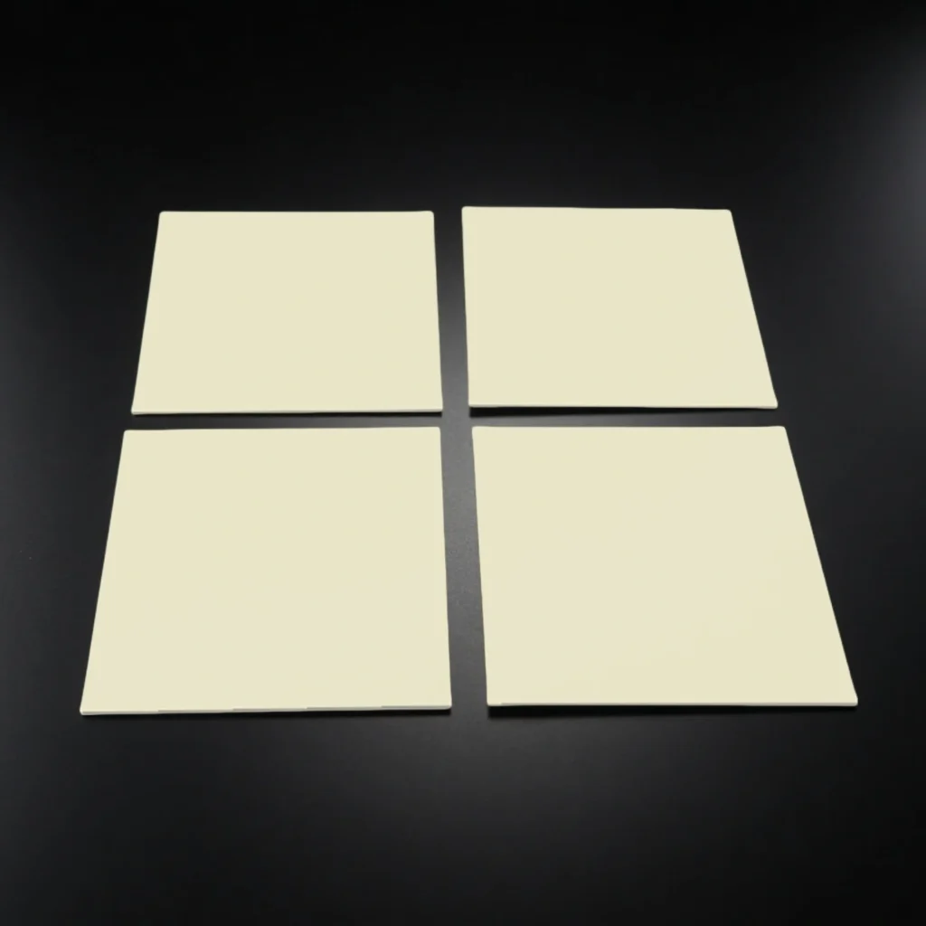
Surface finish decides which circuit process an alumina substrate can support. Thick-film printing normally runs on as-fired 95% surfaces, while thin-film and RF circuits need lapped or polished 99.5%–99.6% substrates with low, uniform roughness. One-side or two-side polishing is selected from your process and handling requirements.
As-Fired
— Standard surface for thick-film printing and general carriers; most economical for volume production.
Lapped
— Improved flatness and roughness control for precision assembly and tighter printing tolerances.
Polished (1-side / 2-side)
— Low-Ra finish for thin-film, RF and fine-line metallization; typical polished roughness is confirmed per grade at engineering review.
When to Choose Alumina Substrates for Your Application?
Alumina substrates are the industry standard for electronic circuits requiring electrical insulation, thermal stability, and precision dimensions. Their combination of stable dielectric properties, moderate thermal conductivity, and cost-effectiveness makes them the most widely used ceramic substrate material.
Alumina Substrates Are the Best Choice When
| Your Application Requirement | Why Alumina Substrates Excel | Recommended Configuration |
|---|---|---|
| RF / microwave circuits (up to 20 GHz) | Stable dielectric constant (9.4-9.8); low loss tangent(<0.0001 at 1 MHz); proven GHz performance | 99.5% or 99.7%; thin (0.3-0.5mm); polished |
| LED packaging & thermal management | Thermal conductivity 18-42 W/m·K; excellent heat spreading; CTE matched to common die materials | 96% or 99%; 1-2mm; metallized |
| PCB prototyping & hybrid circuits | Better thermal stability than FR-4; supports thick/thin film printing; precision dimensions | 96% for cost; 99% for performance; 1-2mm |
| Power module carriers (DBC) | High dielectric strength (15-22 kV/mm); supports direct bond copper; cost-effective vs AlN | 96%; ≥1mm; DBC metallized |
| Sensor substrates | Chemical inertness; stable in harsh environments; supports precise electrode patterns | 99% or 99.7%; custom thickness |
| Thick film circuits | Excellent surface finish for screen printing; withstands firing temperatures | 96%; 0.5-1mm; polished one side |
| Laboratory R&D / prototyping | Fast availability; flexible sizing; cost-effective for experiments | Stock sizes; various purities |
| Cost-sensitive high-volume production | Lowest cost among ceramic substrates; mature supply chain; proven reliability | 96%; standard sizes |
When Alumina Substrates May Not Be Optimal
If any of the cases below match your process, our engineers can recommend a better-fit ceramic option.
needed (>100 W/m·K)
consider aluminum nitride (AlN) substrates
with ultra-low loss
contact us about specialized materials
needed
consider silicon nitride substrates
Why Choose Alumina Over Other Ceramic Substrates?
Alumina is the most widely used ceramic substrate material due to its optimal balance of performance and cost. Here’s when alumina is the right choice:
💡 Selection Tip: Start with 96% alumina for cost-sensitive applications. Move to 99% or 99.7% when you need better dielectric performance or higher purity. Only consider AlN when thermal conductivity >100 W/m·K is essential for your design.
Choose alumina when thermal conductivity demand is moderate.
- For many designs, thermal conductivity of 20–30 W/m·K is sufficient. In these cases, alumina can deliver the required heat transfer at a much lower cost, typically 3–5× lower than AlN for moderate heat loads.
Choose alumina when dielectric reliability matters.
- Alumina provides a stable dielectric constant of around ~9.6 with low loss tangent, making it suitable for many electronic and RF designs. It also offers proven performance at frequencies up to 20+ GHz, supported by extensive design data.
Choose alumina when budget and scalability are priorities.
- Alumina is one of the most cost-effective ceramic substrates for high-volume production. Its mature global supply chain helps control cost while supporting stable sourcing.
Choose alumina when practical availability matters
- Standard alumina formats run on mature, high-volume production lines, so common sizes are usually quicker to source than specialty ceramics. Confirm current availability for your exact size and surface at RFQ.
Choose alumina when flexible processing is needed.
- Alumina supports a wide range of mature secondary processes, including metallization, drilling, polishing, and DBC-related processing. Its well-established manufacturing ecosystem makes it easier to source and process at scale.
Choose alumina when material safety is a concern.
- Unlike BeO, alumina is non-toxic and does not require special handling in normal production environments, making it a safer and simpler material choice.
Looking for the right alumina substrate grade or thickness for your project?
From 96% to 99.7% purity and from thin-film carriers to thick substrates, ADCERAX offers engineered solutions that match RF, LED, and power applications. Explore the categories below to find the substrate that fits your design.
Alumina Ceramic Substrate Applications
Alumina (Al2O3)ceramic substrates are essential in electronics, RF circuits, LED packaging, and research labs. They combine dielectric stability, heat dissipation, and precision machining, making them reliable for both industrial production and advanced R&D.

🔌Electronics & PCB Prototyping
Pain Points: Organic laminates (e.g., FR4) warp under heat, poor dielectric stability causes circuit failures, and inconsistent thickness leads to rework in prototyping.
Our Solution: ADCERAX alumina PCB substrates hold ±0.1 mm thickness (±0.05 mm on review) and dielectric strength typically 15–22 kV/mm, so thick-film printing and assembly stay consistent from prototype to mass production.
Typical grade: 96% as-fired, 0.5–1.0 mm.

📡 RF & Microwave Packaging
Pain Points: High-frequency circuits often suffer from signal degradation, high insertion loss, and unstable dielectric performance, especially in 5G and radar modules.
Our Solution: ADCERAX RF alumina substrates hold a stable dielectric constant (~9.9 typical, 1 MHz) with low loss tangent and lapped/polished surfaces, keeping signal loss low and stable across GHz frequencies. Thin 0.3–0.5 mm substrates with metallization suit compact RF integration.
Typical grade: 99.5%–99.6% polished, 0.3–0.5 mm.
💡 LED & Power Devices
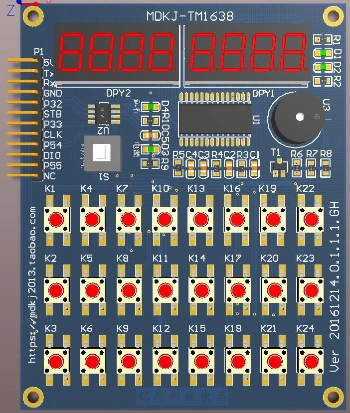
Pain Points: High-power LEDs and power modules face overheating, reduced efficiency, and shortened device lifetime when using low thermal conductivity carriers.
Our Solution: With thermal conductivity typically 20–29 W/m·K, ADCERAX alumina spreads heat from LED and power devices while keeping electrical isolation, supporting longer, more stable operation. For high power-density designs above ~100 W/m·K we recommend AlN instead.
Typical grade: 96%–99%, 1–2 mm, metallization on request.
🔬 Laboratory & R&D
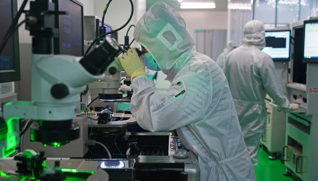
Pain Points: Researchers need small-batch, high-purity substrates for experiments, but often face long lead times, inconsistent quality, and lack of customization.
Our Solution: ADCERAX supplies thin, polished alumina substrates for sensors, thin-film deposition and test boards, with small batches and drawing-based review — so labs can prototype quickly and scale to production.
Typical grade: stock sizes, purity per experiment; polished on request.
Explore Our Alumina Substrate Solutions
From RF circuits and LED packaging to power devices and sensors, our Al2O3 ceramic substrates are engineered for performance and reliability.
customize alumina ceramic substrates supplier
From prototypes to mass production, ADCERAX provides tailor-made alumina ceramic substrates—flexible in size, purity, and machining—to match your application. Lead time for custom prototype: approx. 7-25days; mass orders: 3-10 weeks
Customization Options
Extra-large / Extra-small diameters, non-standard thicknesses, and ultra-long / ultra-short lengths.
Provide higher - level dimensional accuracy and concentricity control than the standard.
Flanges, steps, threads, drilling holes, grooves, etc.
Adjust the material according to the application requirements.
Polish and grind the surface to achieve a specific surface roughness.
Customization Process
Send your drawing, CAD file, or sample with material, dimensions, tolerances, and quantity. Our engineers will review it and provide a quotation with lead time and pricing.
Once the quote is approved, we proceed with sample prototyping (1–50 pcs) if needed, for testing and validation.
After approval, we begin batch production with CNC machining, sintering, and polishing. All parts are inspected for dimensions, purity, and surface finish.
Finished products are securely packed and shipped via DHL/FedEx/UPS or your preferred method. We support global delivery with full documentation.
Why Choose ADCERAX as Your Alumina Ceramic Substrate Manufacturers?
ADCERAX is a trusted alumina ceramic substrate factory in China, delivering factory-direct pricing, fast lead times, and full customization. With strict tolerance control and reliable global shipping, we make sourcing Al2O3 substrate simple, consistent, and worry-free.
Factory-direct alumina substrates with grade, flatness and surface checks on every production batch.
Grade, surface and metallization advice from prototype to volume production.
Small batches to volume runs, with custom sizes, holes and metallization.
Common sizes reviewed quickly; custom substrates typically 3–7 weeks.
China Alumina Ceramic Substrate Factory-ADCERAX

ADCERAX is a professional China alumina substrate manufacturer and supplier that offers high-performance components with tight tolerances (±0.1mm) and custom geometries. Using advanced forming methods and CNC machining, we deliver precision-engineered solutions for electronics, chemical, and high-temperature applications.
- 99.7% high-purity alumina for stable performance
- Custom parts based on your drawings or samples
- Fast prototyping (7–15 days) & flexible MOQ
- ISO-compliant quality control & inspection reports
- Direct engineering support from design to delivery
Alumina Substrate Etching and Machining
We deliver customized alumina ceramic substrates solutions to meet diverse industrial needs with precision and reliability.
| Processing Type | Options | Typical Specification |
|---|---|---|
| Surface Finish | As-fired, lapped, polished (1-side or 2-side) | Ra 0.1-0.8 μm (polished) |
| Metallization | Mo-Mn, Ni/Au, Cu (DBC), Ag, sputtered layers | Per customer spec |
| Laser Drilling | Through holes, blind vias, slots | Min Ø0.1mm; ±0.05mm position |
| Dicing / Cutting | Laser cutting, diamond scribing, precision dicing | ±0.05mm |
| Thickness Tolerance | Standard / Tight | ±0.1mm (std) / ±0.05mm (tight) |
Metallization routes (thick-film print, plating, DBC/DPC-related processing) are confirmed case-by-case through engineering review of your pattern, layer stack and reliability requirements.
Frequently Asked Questions
Technical answers to help you specify, source, and use alumina ceramics substrate effectively.
Why is alumina a good substrate?
It combines stable dielectric constant (~9.6), low loss tangent, moderate thermal conductivity, and strong mechanical strength with high-temperature capability and dimensional stability.
96% or 99.6% alumina substrate — which grade do I need?
As an industry convention, 96% alumina with an as-fired surface is the standard choice for thick-film printing and general ceramic PCB carriers, while 99.6% alumina with a lapped or polished surface is the standard for thin-film, RF and fine-line circuits that need low, uniform roughness. If you share your circuit process, roughness target and metallization plan, we confirm the grade in an engineering review before quotation.
Alumina substrate vs FR-4 — what's the key difference?
Alumina maintains dielectric and mechanical stability at high temperatures where FR-4 softens; it also offers better heat spreading and lower RF loss for many high-frequency designs.
How do I choose the right alumina substrate thickness?
Thin substrates (0.3–0.5 mm) are ideal for lightweight circuits and prototyping, while standard substrates (1–2 mm) fit PCB carriers and LED boards. For high-power devices and heat spreaders, thick substrates (≥3 mm) provide stability and efficient heat dissipation.
What methods are used for alumina substrate etching?
Common methods include laser etching, chemical etching, grinding, and thin-film patterning, depending on the design and precision required. Laser etching is widely used for fine features and markings, while photolithography and chemical etching are often applied to metallized layers rather than the alumina itself. ADCERAX supports custom alumina substrate etching and machining from drawings or prototypes, with tolerance control up to ±0.05 mm, for both R&D batches and production orders.
Do you supply metallized or DBC copper alumina substrates?
Metallized alumina substrates are supported through engineering review. Thick-film printed, plated and bonded-copper (DBC-related) routes are confirmed case-by-case from your pattern, layer stack, and reliability requirements — please send a drawing or Gerber file so we can confirm feasibility and lead time.
How should I clean Al₂O₃ substrates before use?
Wipe with IPA or acetone in a clean tray, then DI water rinse and nitrogen blow-dry. Avoid abrasive cloths; handle with gloves to prevent fingerprints that affect metallization or printing.
How can I get a quotation for alumina substrates?
To provide an accurate quotation, please share substrate dimensions, purity level, thickness, surface treatment (polished, metallized, etc.), and order quantity. Our team will respond within 24 hours with a detailed quote.
What to Send for an Alumina Substrate Quote
To quote a custom alumina substrate, send what you have:
- Grade / purity: 95% / 96% / 99% / 99.5% / 99.6%–99.7%
- Dimensions: length, width, thickness, and tolerance
- Surface: as-fired / lapped / polished (Ra target)
- Holes, slots or laser-scribing; metallized or bare
- Thermal / electrical requirement and application
- Drawing, Gerber/DXF, photo or old-part sample; quantity
Alumina substrates serve thick-film, thin-film, RF, LED and power circuits. Send your details and our engineers will review the fit before quoting.
*Our team will answer your inquiries within 24 hours.
*Your information will be kept strictly confidential.
info@adcerax.com
Tel:+86-0731-84428843
WhatsApp:+86 19311583352
Within 24 hours