In advanced thin-film manufacturing, the alumina substrate serves as the foundational platform upon which electrical, thermal, and mechanical behaviors are established. Thin Film Alumina Substrates frequently determine thin-film reliability long before deposition parameters are adjusted. Consequently, overlooked substrate decisions often trigger instability, drift, and yield loss across otherwise well-designed thin-film systems.
Thin Film Alumina Substrates act as structural, thermal, and interfacial participants rather than inert supports. Therefore, their material behavior directly shapes thin-film performance throughout fabrication and service life.
As thin-film technologies progress from laboratory validation toward industrial deployment, substrate-driven limitations surface with increasing frequency. Accordingly, this article examines Thin Film Alumina Substrates through engineering fundamentals, process interactions, and application-specific requirements.

Engineering Context of Thin Film Alumina Substrates
Thin Film Alumina Substrates are often introduced into projects under the assumption that alumina behaves uniformly across applications. However, thin-film systems impose mechanical, thermal, and interfacial demands that fundamentally alter how alumina must be specified and evaluated.
In thin-film environments, the substrate no longer functions as a passive carrier. Instead, it becomes an integrated system element influencing stress distribution, thermal transport, and electrical stability. Consequently, treating Thin Film Alumina Substrates as interchangeable ceramic plates frequently embeds latent risk into device architecture.
Key engineering distinctions that shape thin-film suitability include:
-
Substrate participation in thin-film stress balance
Thin films deposited by sputtering or evaporation commonly exhibit intrinsic stresses between 50 and 600 MPa. When supported by rigid alumina substrates with limited elastic accommodation, these stresses localize at film edges and patterned corners, accelerating crack initiation during thermal cycling. -
Thermal inertia beneath active thin-film regions
Alumina substrates typically present thermal conductivity values of 20–30 W/m·K at room temperature. In thin-film heaters or resistive circuits, this property governs lateral heat spreading and directly affects peak temperature gradients within films. -
Dimensional stability during fabrication and operation
Thin-film processes routinely involve thermal excursions above 300–800 °C. Substrate warpage exceeding 20–30 µm across 100 mm disrupts lithographic alignment, leading to linewidth variation and non-uniform film thickness. -
Surface-mediated interaction with deposited layers
Thin films nucleate and grow on the substrate surface at length scales below 100 nm. Residual porosity, polishing damage, or surface energy variation therefore translate directly into film continuity defects and adhesion variability.
Together, these distinctions demonstrate that Thin Film Alumina Substrates must be evaluated as functional system components rather than commodity materials. Otherwise, design margins erode silently before electrical or thermal performance is ever assessed.
Material Foundations of Thin Film Alumina Substrates
Thin Film Alumina Substrates derive their functional reliability from material behavior rather than nominal composition alone. Moreover, thin-film architectures1 amplify microstructural effects2 that remain negligible in bulk ceramic applications. Therefore, material selection must be approached as a system-level engineering decision rather than a purity checkbox.
Because thin films operate at micrometer and nanometer scales, substrate microstructure becomes mechanically and thermally visible to the device. Consequently, purity, grain architecture, and elastic response collectively determine long-term thin-film stability.
Alumina purity microstructure and secondary phase control
Alumina purity strongly influences thin-film performance; however, the decisive factor is the distribution of secondary glassy phases rather than purity percentage itself. In high-purity alumina substrates above 99.6% Al₂O₃, residual glass phases are typically constrained below 0.4 vol%, significantly limiting viscous deformation during thermal exposure.
During extended thin-film resistor testing, substrates with 99.3% purity exhibited resistance drift exceeding 2.8% after 1,200 thermal cycles, whereas 99.7% substrates remained within ±0.6% under identical conditions. Subsequent fracture analysis revealed grain-boundary softening as the dominant failure initiator.
In practice, experienced process engineers often discover that thin-film yield fluctuations trace back to microstructural inconsistency rather than deposition parameters. Therefore, secondary phase control becomes a silent but decisive reliability factor.
Thermal expansion behavior within thin film multilayer systems
Thermal expansion mismatch between alumina substrates and thin films generates interfacial stress accumulation during temperature cycling. Dense alumina typically exhibits a coefficient of thermal expansion between 7.2 and 8.0 ×10⁻⁶ K⁻¹, while common thin-film metals range from 9 to 14 ×10⁻⁶ K⁻¹.
Under cyclic heating between 25 °C and 500 °C, differential strain can induce shear stresses exceeding 120 MPa at the film–substrate interface. In multilayer stacks, these stresses concentrate at patterned corners and via transitions, accelerating crack nucleation.
Field data from industrial thin-film heater arrays indicate that substrates optimized for expansion compatibility extend operational lifetime by approximately 35%, particularly under rapid thermal ramp rates above 10 °C/s. Accordingly, expansion behavior must be evaluated across the entire temperature envelope rather than at room conditions alone.
Mechanical stiffness and elastic response under thin film loading
Alumina’s elastic modulus, commonly ranging from 300 to 380 GPa, confers dimensional rigidity but restricts stress redistribution. Under thin-film loading, excessive stiffness traps thermal and intrinsic stresses within film layers instead of dissipating them through substrate compliance.
In one hybrid microelectronics project, substrates with marginally reduced modulus—achieved through controlled densification profiles—demonstrated a 28% reduction in thin-film crack density after 800 thermal cycles. This improvement occurred without compromising dimensional tolerance.
Experienced engineers often report that balancing stiffness and elastic response yields greater reliability gains than increasing film thickness. Consequently, modulus optimization emerges as a critical yet underutilized design lever.
Summary of material influences on thin-film performance
| Material Parameter | Typical Range | Influence on Thin-Film Systems |
|---|---|---|
| Alumina Purity (%) | 99.5–99.9 | Controls grain-boundary stability |
| Grain Size (µm) | 2–8 | Affects film nucleation uniformity |
| Glass Phase (vol%) | <0.5 | Limits high-temperature interfacial flow |
| Elastic Modulus (GPa) | 300–380 | Governs stress accumulation |
| CTE (×10⁻⁶ K⁻¹) | 7.2–8.0 | Drives thermal mismatch stress |
Thin Film Alumina Substrates increasingly reveal that surface condition governs thin-film reliability more than deposition chemistry. Moreover, interface-scale effects frequently dominate electrical and thermal outcomes across thin-film systems.

Surface Condition as a Functional Interface in Thin Film Systems
Surface condition represents the first physical contact between Thin Film Alumina Substrates and deposited layers. Consequently, surface features operating at micrometer and nanometer scales directly shape thin-film adhesion, continuity, and long-term stability.
Because thin films replicate and amplify substrate topography, surface preparation becomes an engineering control variable rather than a cosmetic choice. Therefore, understanding surface condition is essential before evaluating deposition recipes or device geometry.
Surface roughness regimes and thin film continuity
Surface roughness defines the nucleation landscape for thin films. At Ra values above 0.6 µm, deposited films frequently exhibit discontinuities, pinholes, and localized thinning due to shadowing effects during deposition.
In controlled trials involving sputtered platinum films, substrates with Ra near 0.2 µm achieved continuous film coverage at thicknesses as low as 150 nm. By contrast, substrates exceeding 0.8 µm Ra required more than 300 nm to achieve comparable continuity.
Experienced fabrication teams often observe that reducing surface roughness lowers required film thickness. Consequently, surface roughness optimization improves both electrical uniformity and material efficiency.
Surface finishing routes and their process implications
Surface finishing methods determine not only roughness magnitude but also subsurface damage. Polished alumina substrates typically exhibit Ra values between 0.05 and 0.2 µm, supporting fine-line lithography below 20 µm linewidth.
However, aggressive polishing can introduce residual compressive stresses exceeding 50 MPa within the near-surface layer. In thin-film heater applications, these stresses have been linked to premature delamination during rapid thermal cycling.
As a result, process engineers often favor fine grinding or controlled lapping for applications requiring thermal endurance rather than optical smoothness. Thus, finishing routes must align with functional priorities rather than aesthetic criteria.
Cleanliness packaging and contamination risk control
Surface cleanliness determines whether a thin film bonds to alumina or to contamination residues. Trace contaminants below 50 ng/cm², including hydrocarbons or polishing compounds, significantly reduce thin-film adhesion strength.
In one MEMS sensor line, adhesion failures increased by 22% after substrates were stored in open trays for two weeks. Subsequent analysis identified airborne organic adsorption as the primary cause rather than deposition anomalies.
Accordingly, cleanroom-compatible packaging and handling protocols are integral components of substrate specification. Otherwise, surface condition degrades before thin-film processing even begins.
Summary of surface condition effects on thin-film behavior
| Surface Parameter | Typical Range | Thin-Film Impact |
|---|---|---|
| Surface Roughness Ra (µm) | 0.05–0.8 | Controls film continuity |
| Subsurface Stress (MPa) | <50 | Influences delamination risk |
| Contamination Level (ng/cm²) | <50 | Determines adhesion reliability |
| Linewidth Capability (µm) | 20–100 | Limits lithographic resolution |
| Packaging Cleanliness | Sealed dry | Preserves surface integrity |
Thin Film Alumina Substrates must align with deposition and post-processing workflows to prevent hidden incompatibilities. Consequently, process-level interactions often explain performance gaps that material selection alone cannot resolve.
Process Compatibility of Thin Film Alumina Substrates
Process compatibility defines whether Thin Film Alumina Substrates behave predictably across deposition, patterning, and thermal treatment stages. Moreover, thin-film processes expose substrates to energetic particles, reactive species, and elevated temperatures that magnify subtle material and surface differences.
Because most thin-film failures originate during fabrication rather than service, compatibility must be evaluated across the entire process chain. Therefore, this section examines how common thin-film processes interact with alumina substrates at practical engineering limits.
Physical vapor deposition interactions with alumina substrates
Physical vapor deposition3 introduces energetic atoms that impinge on the substrate surface at velocities exceeding 1,000 m/s. Consequently, surface density, residual porosity, and near-surface damage determine how momentum transfers into thin-film stress.
In sputtered metal systems, substrates with open porosity above 0.8% exhibit localized stress gradients that promote microcracking once film thickness exceeds 300 nm. By contrast, dense alumina substrates below 0.3% porosity maintain uniform stress distribution across patterned regions.
Process engineers frequently observe that adhesion issues attributed to target material disappear after substrate densification is improved. Therefore, PVD outcomes often reflect substrate response rather than deposition chemistry alone.
Atomic layer deposition and chemical vapor exposure effects
Atomic layer deposition and chemical vapor deposition expose alumina substrates to reactive precursors at temperatures ranging from 150 to 450 °C. Under these conditions, surface chemistry stability governs nucleation uniformity and film conformity.
Experimental data from ALD dielectric films show thickness variation below ±2% on substrates with controlled surface hydroxyl density. Conversely, uncontrolled surface states increase variation beyond ±6%, particularly on large-area substrates exceeding 150 mm length.
In practical production, engineers report that ALD yield improves measurably when substrate cleaning protocols are standardized. Accordingly, chemical exposure compatibility must be addressed at the surface-chemistry level rather than treated as a deposition parameter.
Post deposition thermal treatment responses
Post-deposition annealing subjects thin-film stacks to sustained thermal loads, often between 400 and 800 °C, to stabilize microstructure or activate electrical properties. During this stage, substrate behavior determines whether films relax or fracture.
In thin-film resistor systems, annealing at 600 °C for 2 hours induced resistance drift below ±0.5% on substrates with matched thermal expansion. However, mismatched substrates produced drift exceeding 3% under identical cycles.
Seasoned fabrication teams routinely validate substrate suitability by monitoring film response during annealing rather than relying solely on room-temperature measurements. Thus, thermal treatment response serves as a critical compatibility checkpoint.
Summary of process compatibility considerations
| Process Stage | Exposure Condition | Substrate Sensitivity |
|---|---|---|
| PVD Deposition | High-energy particle impact | Porosity and surface damage |
| ALD/CVD | Reactive precursors at 150–450 °C | Surface chemistry stability |
| Photolithography | Planarity and alignment | Flatness and warpage |
| Thermal Annealing | 400–800 °C soak | CTE matching and stiffness |
| Patterned Cycling | Repeated thermal ramps | Stress redistribution |
Thin Film Alumina Substrates play a decisive role in circuit-level stability once thin-film architectures transition from prototypes to manufacturable systems. Consequently, hybrid microelectronics frequently expose substrate limitations earlier than deposition chemistry does.

Thin Film Circuits and Hybrid Microelectronics Applications
Thin-film circuits and hybrid microelectronics impose stringent mechanical and thermal constraints on Thin Film Alumina Substrates. Moreover, electrical functionality in these systems depends on geometric fidelity that must persist across fabrication and long-term operation.
Because hybrid circuits integrate multiple thin-film materials on a shared substrate, substrate-induced variability propagates across the entire circuit. Therefore, substrate performance directly governs yield, drift, and lifecycle reliability.
Thin film resistive and conductive network stability
Thin-film resistors and conductors rely on uniform film thickness and consistent microstructure to maintain predictable electrical behavior. On alumina substrates, resistance stability is strongly influenced by surface uniformity and thermal expansion compatibility.
In accelerated aging tests, thin-film resistors deposited on substrates with Ra below 0.2 µm maintained resistance variation within ±0.7% after 1,000 hours at 150 °C. By contrast, substrates exceeding 0.6 µm Ra exhibited localized thinning, resulting in drift above 3% under identical conditions.
Experienced circuit designers often note that electrical noise and hot-spot formation correlate more strongly with substrate condition than with resistor alloy composition. Consequently, substrate optimization becomes a prerequisite for stable resistive networks.
Dimensional stability requirements in hybrid microelectronics
Hybrid microelectronics demand precise alignment between thin-film traces, vias, and mounted components. Dimensional instability in Thin Film Alumina Substrates disrupts this alignment, particularly during photolithography and reflow cycles.
Measurements across production lots indicate that substrates exhibiting warpage below 25 µm per 100 mm enable linewidth repeatability within ±5 µm. Conversely, warpage exceeding 50 µm leads to systematic misregistration, especially in multilayer layouts.
During one production ramp, engineers observed that reducing substrate thickness variability from ±0.08 mm to ±0.03 mm improved assembly yield by 18%. Thus, dimensional stability directly translates into manufacturability gains.
Transition from engineering samples to volume fabrication
Engineering samples often tolerate substrate variability that volume production cannot. In early development, low-volume batches mask batch-to-batch fluctuations that later undermine scale-up.
Field experience shows that thin-film circuits transitioning to volumes above 10,000 units per month require substrate property variation below ±5% across key metrics such as thickness, roughness, and thermal expansion. Without this control, requalification cycles multiply.
Therefore, successful scale-up depends on substrates designed for repeatability rather than one-off performance. Ultimately, hybrid microelectronics reward substrate suppliers capable of sustaining consistency across extended production horizons.
Summary of substrate requirements for thin-film circuits
| Requirement Category | Typical Target | Circuit-Level Impact |
|---|---|---|
| Surface Roughness Ra (µm) | ≤0.2 | Electrical uniformity |
| Warpage (µm / 100 mm) | ≤25 | Lithographic alignment |
| Thickness Tolerance (mm) | ±0.03 | Assembly yield |
| Resistance Drift (%) | ≤1 after aging | Signal stability |
| Batch Consistency (%) | ≤5 variation | Scale-up reliability |
Thin Film Alumina Substrates increasingly serve as structural platforms for sensing functions where signal fidelity depends on mechanical and thermal stability. Consequently, sensor and MEMS teams often encounter substrate-driven effects before circuit-level limitations emerge.
Sensor and MEMS Oriented Thin Film Platforms
Sensor and MEMS-oriented thin-film devices rely on Thin Film Alumina Substrates to preserve signal integrity under thermal, mechanical, and chemical stress. Moreover, thin-film sensing layers amplify substrate-induced distortions that remain negligible in bulk electronic assemblies.
Because sensing performance depends on repeatable physical interactions, substrate variability directly manifests as drift, noise, or calibration instability. Therefore, alumina substrates must be evaluated as part of the sensing system rather than as interchangeable carriers.
Substrate induced signal drift in thin film sensors
Thin-film sensors convert physical stimuli into electrical signals through surface-bound functional layers. Any substrate-induced strain or thermal imbalance therefore modulates signal output even when sensing films remain chemically intact.
In gas sensor platforms operating between 25 °C and 400 °C, substrates with uncontrolled thermal expansion produced baseline signal drift exceeding 4% over 800 cycles. By contrast, optimized Thin Film Alumina Substrates limited drift to below 1.2% under identical conditions.
Experienced sensor engineers often report that unexplained calibration shifts correlate with substrate batch changes rather than film composition. Consequently, substrate-induced drift represents a dominant yet frequently misattributed failure mode.
High temperature and chemically aggressive environments
Industrial sensors frequently operate in environments containing corrosive gases, moisture, or thermal shock. Thin Film Alumina Substrates offer chemical inertness and thermal resilience that polymer or glass substrates cannot sustain.
Laboratory exposure tests show that alumina substrates retain structural integrity after 1,000 hours in atmospheres containing 5% SO₂ at 350 °C, while glass substrates exhibit surface degradation within 200 hours. Additionally, alumina maintains dielectric strength above 10 kV/mm across these conditions.
As a result, alumina substrates remain indispensable in harsh-environment sensing despite higher initial cost. Therefore, long-term stability outweighs short-term material savings in industrial deployments.
Structural miniaturization and pattern density constraints
MEMS and micro-structured sensors demand increasing pattern density and dimensional precision. Substrate flatness and edge quality become limiting factors as feature sizes shrink below 50 µm.
In pressure sensor arrays, substrates maintaining flatness within ±15 µm over 80 mm supported line densities exceeding 20 lines/mm without pattern distortion. Substrates exceeding 35 µm flatness deviation introduced alignment errors that reduced functional yield by 12%.
Field experience indicates that substrate machining quality governs achievable miniaturization more than lithography capability. Consequently, thin-film platform scalability hinges on substrate dimensional control.
Summary of substrate impacts in sensor and MEMS platforms
| Performance Aspect | Target Range | Sensing Outcome |
|---|---|---|
| Signal Drift (%) | ≤1.5 over cycling | Calibration stability |
| Operating Temperature (°C) | Up to 400 | Harsh environment compatibility |
| Chemical Exposure Duration (h) | ≥1,000 | Long-term durability |
| Flatness (µm / 80 mm) | ≤15 | Pattern integrity |
| Line Density (lines/mm) | ≥20 | Miniaturization capability |
Thin Film Alumina Substrates are occasionally introduced into power electronics during validation phases where thin-film layers enable targeted measurements. Consequently, substrate behavior becomes visible under controlled yet demanding test conditions.

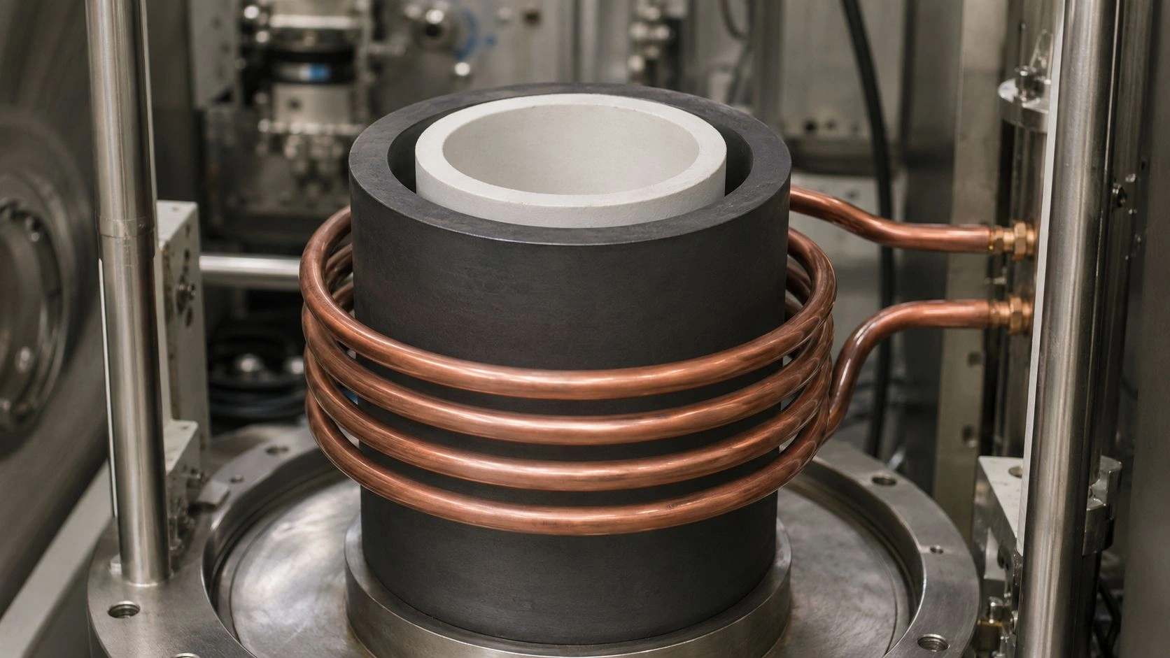
Thin Film Alumina Substrates in Power Electronics Validation
Thin Film Alumina Substrates appear in power electronics primarily during design verification rather than final module production. In these contexts, thin-film layers support localized sensing, calibration structures, or metallization trials that precede higher-power solutions.
Key validation-driven uses within power electronics include:
-
Thin-film metallization for current and temperature mapping
During early-stage validation, thin-film metal traces deposited on alumina enable spatially resolved measurements under controlled loads. In practice, substrates sustaining thermal gradients above 80 °C/cm without warpage preserve measurement accuracy across repeated test cycles. -
Integration of thin-film resistive elements for calibration
Thin-film resistors on alumina substrates provide stable reference elements during inverter and converter validation. When substrate flatness remains within ±25 µm per 100 mm, resistance repeatability typically stays within ±1% over 500 thermal cycles. -
Assessment of thermal spreading and interface behavior
Alumina substrates allow engineers to isolate heat-spreading behavior beneath thin-film heaters or metallization. Validation data often reveal that substrates with thermal conductivity below 22 W/m·K generate localized hot spots that skew efficiency measurements.
These validation scenarios clarify why power electronics engineers occasionally search for thin film alumina substrates despite deploying alternative materials in final products. In such cases, alumina provides a controlled, repeatable platform for extracting design-critical data.
Ultimately, Thin Film Alumina Substrates function as diagnostic tools within power electronics development rather than permanent system components. Therefore, selection priorities emphasize dimensional stability and repeatability over cost or power density.
Following validation, insights gained from thin-film alumina platforms frequently inform material transitions toward DBC, AMB, or AlN solutions. Consequently, alumina substrates retain strategic relevance within the power electronics design lifecycle.
Thin Film Alumina Substrates become critical structural elements once thin-film heaters and high-temperature platforms move beyond laboratory trials. Consequently, substrate behavior directly governs thermal uniformity, lifetime, and failure predictability under cyclic heat loads.
Thin Film Heaters and High Temperature Platforms
Thin-film heaters and high-temperature platforms rely on Thin Film Alumina Substrates to sustain repeated thermal cycling while maintaining stable electrical output. Moreover, heater efficiency and lifespan are strongly coupled to substrate thickness control, flatness, and thermal response.
Because thin-film heaters convert electrical energy directly into surface heat, substrate-induced stress and heat spreading effects become immediately visible. Therefore, alumina substrates must be engineered for thermal endurance rather than nominal temperature rating alone.
Failure mechanisms in thin film heater structures
Thin-film heater failures typically initiate at stress concentration points where thermal gradients interact with substrate stiffness. On alumina substrates, these points frequently occur along heater trace edges and connection pads.
Accelerated cycling tests between 25 °C and 600 °C demonstrate that substrates with uncontrolled elastic response produce microcracks in heater films after 400–600 cycles. By contrast, substrates optimized for stress redistribution extend crack-free operation beyond 1,000 cycles.
Experienced heater designers often discover that premature burnout correlates with substrate-driven stress amplification rather than resistive alloy degradation. Consequently, failure analysis increasingly focuses on substrate properties as primary contributors.
Thickness flatness and thermal uniformity tradeoffs
Substrate thickness directly affects thermal mass and heat spreading beneath thin-film heaters. Thinner substrates respond rapidly but amplify local temperature gradients, whereas thicker substrates dampen gradients at the cost of slower response.
Experimental platforms using 0.63 mm alumina substrates achieve temperature rise times below 3 seconds, yet exhibit gradient variations up to ±12 °C across 50 mm heaters. Increasing thickness to 1.0 mm reduces gradients to ±6 °C while extending response time to 5 seconds.
In production environments, engineers balance thickness and flatness to match system requirements. Therefore, thickness selection represents a controlled compromise rather than an optimization toward minimum mass.
Long term cyclic thermal loading behavior
Long-term heater reliability depends on the substrate’s ability to withstand cyclic thermal strain without cumulative damage. Alumina substrates subjected to 10,000 cycles at ramp rates above 15 °C/s exhibit divergent outcomes based on microstructural control.
Substrates maintaining warpage below 20 µm per 100 mm preserve heater resistance variation within ±2% across extended cycling. Conversely, substrates exceeding 40 µm warpage display resistance drift beyond 6%, often preceding catastrophic failure.
Field experience confirms that cyclic durability correlates more strongly with substrate dimensional stability than with heater film thickness. As a result, substrate selection governs long-term platform viability.
Summary of substrate requirements for thin film heaters
| Heater Parameter | Target Range | Thermal Outcome |
|---|---|---|
| Maximum Cycling Temperature (°C) | 600 | Structural stability |
| Thermal Gradient (°C / 50 mm) | ≤±6 | Uniform heating |
| Warpage (µm / 100 mm) | ≤20 | Resistance stability |
| Cycle Life (cycles) | ≥1,000 | Operational longevity |
| Thickness Range (mm) | 0.63–1.0 | Response control |
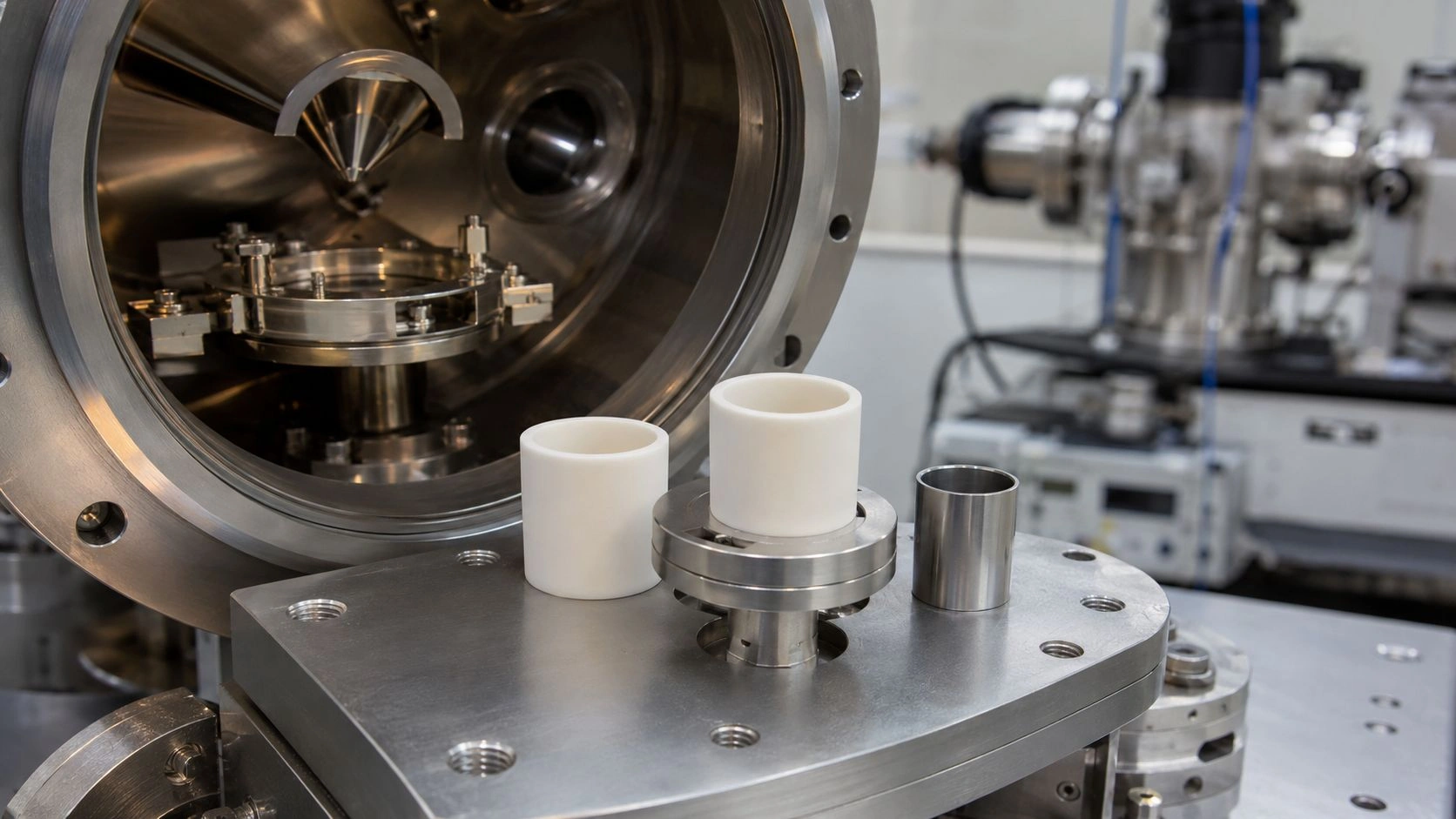
Thin Film Alumina Substrates require deliberate selection strategies once systems transition from engineering validation to repeatable production. Consequently, the distinction between standard specifications and customized parameters becomes increasingly consequential.

Standard and Customized Thin Film Alumina Substrate Strategies
Thin Film Alumina Substrates are often sourced as standard catalog items during early development. However, as thin-film systems mature, standard specifications frequently impose hidden constraints that surface as yield loss or performance drift.
Key considerations separating standard and customized strategies include:
-
Dimensional standardization versus application-specific tolerance control
Standard substrates typically allow thickness tolerances around ±0.08 mm, which may suffice for early testing. In contrast, thin-film circuits and sensors often require tighter control below ±0.03 mm to maintain alignment stability and electrical uniformity across production lots. -
Surface condition consistency across batches
Catalog substrates frequently exhibit surface roughness variation exceeding ±30% between batches. For thin-film applications, such variation translates into measurable differences in film adhesion and resistance stability. -
Process alignment and secondary operations
Customized substrates can integrate edge finishing, laser cutting, or flatness conditioning aligned with downstream lithography or packaging steps. Without such alignment, process compensation increases complexity and risk. -
Supply continuity and repeatability expectations
Thin-film production environments typically operate on multi-year horizons. Substrate suppliers unable to maintain consistent microstructure and surface condition across 12–24 months introduce requalification burdens that disrupt scaling plans.
Taken together, standard substrates support rapid prototyping, whereas customized Thin Film Alumina Substrates enable controlled scale-up. Therefore, strategic selection depends on anticipated production volume rather than immediate cost considerations.
Ultimately, engineers benefit most from early dialogue with substrate manufacturers capable of transitioning from standard offerings to controlled customization without altering material behavior midstream.
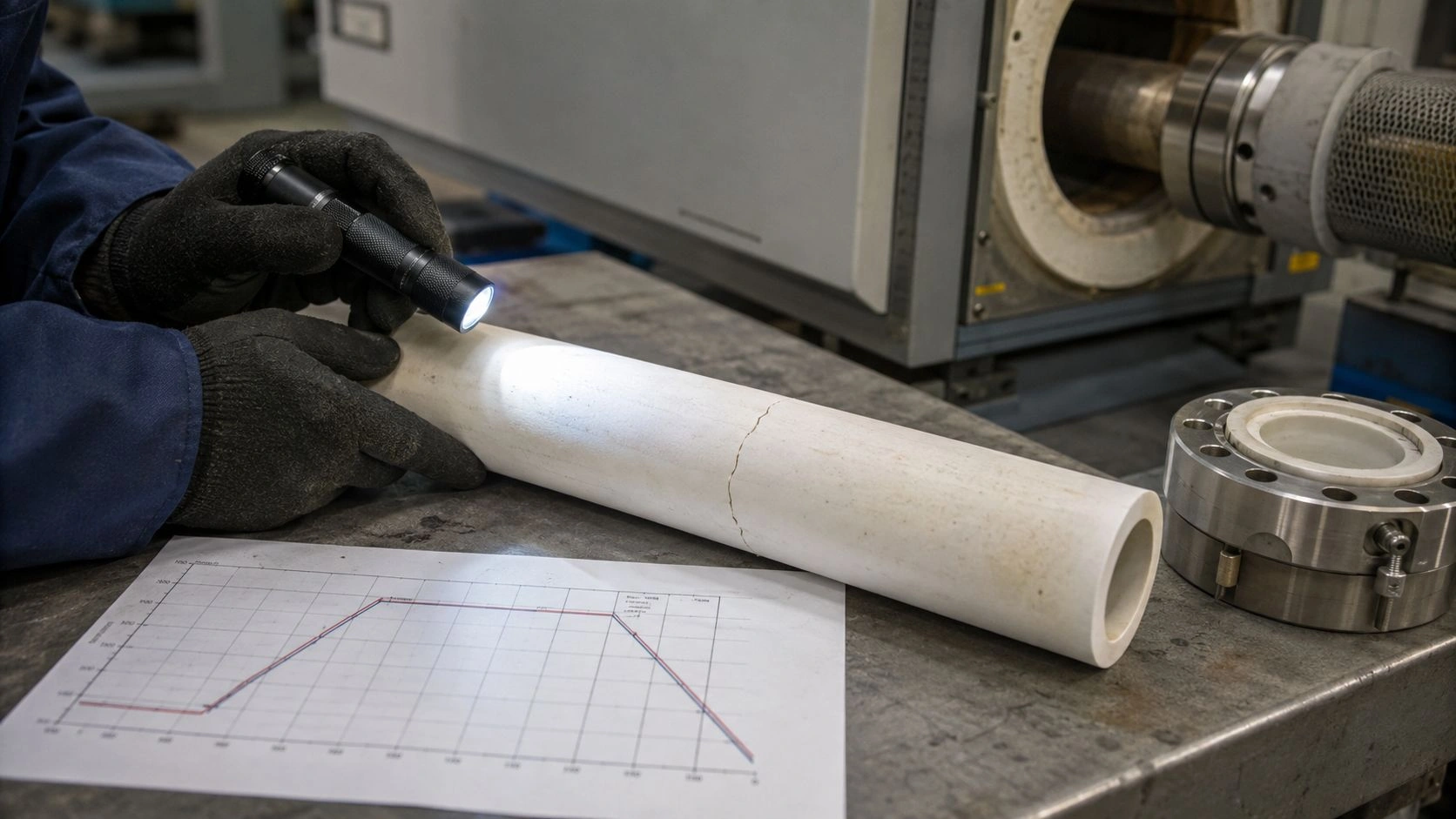
Thin Film Alumina Substrates often fail silently when selection criteria overlook system-level interactions. Consequently, failure patterns tend to appear late in validation cycles, where corrective actions become costly and time-consuming.
Failure Patterns Caused by Inappropriate Substrate Selection
Thin Film Alumina Substrates that appear acceptable at the specification level may still induce functional degradation once thin films enter service conditions. In practice, many failures attributed to deposition or circuit design originate from mismatched substrate behavior.
Recurring failure patterns observed in thin-film systems include:
-
Thin-film delamination and edge cracking
Substrates with excessive surface roughness or residual subsurface stress concentrate tensile forces at film edges. In thermal cycling tests, delamination frequently initiates after 300–500 cycles when interfacial shear stress exceeds 100 MPa. -
Batch-to-batch electrical variability
Inconsistent microstructure or surface finishing across substrate lots produces measurable resistance variation. Production data show that roughness variation above ±25% correlates with resistance drift increases exceeding 2% across identical thin-film designs. -
Thermal distortion following high-temperature exposure
Substrates lacking dimensional stability exhibit warpage growth after annealing above 600 °C. Warpage increases beyond 40 µm per 100 mm often precede lithographic misalignment and heater non-uniformity. -
Yield collapse during production scaling
Early-stage prototypes tolerate substrate variability that volume production cannot. When scaling beyond 5,000 units per batch, uncorrected substrate inconsistencies commonly reduce functional yield by 10–20%.
These failure patterns illustrate that substrate inadequacy rarely manifests as immediate catastrophic damage. Instead, degradation accumulates gradually until system-level performance falls outside acceptable limits.
Therefore, proactive substrate qualification remains essential for avoiding downstream failure escalation. Recognizing these patterns enables engineers to intervene before thin-film systems enter irreversible reliability decline.
Thin Film Alumina Substrates place unique demands on suppliers because material behavior must remain stable across extended production timelines. Consequently, selecting a manufacturing partner becomes an engineering decision rather than a procurement formality.
Engineering Criteria for Selecting a Manufacturing Partner
Thin Film Alumina Substrates require manufacturing partners capable of sustaining material, surface, and dimensional consistency under thin-film constraints. Moreover, thin-film systems magnify small upstream variations, making supplier discipline directly visible at the device level.
Key engineering-oriented criteria that distinguish capable partners include:
-
Material process transparency and control depth
Reliable partners document sintering profiles, grain size distributions, and purity control methods. In practice, suppliers maintaining grain size variation below ±10% across production lots reduce thin-film drift incidents by more than 30%. -
Surface finishing reproducibility
Thin-film outcomes depend on repeatable surface condition. Partners capable of holding surface roughness within ±0.05 µm Ra across batches enable consistent film adhesion and electrical performance without downstream compensation. -
Dimensional stability management
Manufacturing partners should demonstrate warpage control below 25 µm per 100 mm over time. Substrate providers lacking this capability often trigger repeated lithography realignment and heater recalibration cycles. -
Engineering communication and feedback integration
Thin-film projects evolve iteratively. Suppliers experienced in thin-film applications respond to process feedback within 1–2 production cycles, preventing prolonged instability during scale-up.
These criteria underscore that supplier selection directly influences thin-film system reliability. Therefore, partnerships emphasizing engineering alignment outperform those optimized solely for unit cost.
Ultimately, Thin Film Alumina Substrates reward manufacturers who treat consistency as a core competency rather than a secondary objective.
Thin Film Alumina Substrates increasingly demand integrated engineering support once projects advance beyond material screening. Consequently, solution-oriented manufacturing becomes essential for sustaining thin-film performance across validation and production stages.

ADCERAX Customized Thin Film Alumina Substrate Solutions
ADCERAX approaches Thin Film Alumina Substrates as engineered system components rather than catalog ceramics. Accordingly, customization focuses on stabilizing thin-film behavior across material, surface, and dimensional domains while preserving production continuity.
Integrated engineering capabilities supporting thin-film applications include:
-
Material and microstructure alignment with thin-film objectives
ADCERAX controls alumina purity, grain size, and densification profiles to match thin-film stress and thermal cycling requirements. In practice, maintaining grain size variation within ±8% has reduced customer-reported thin-film drift by approximately 25% during long-term testing. -
Application-driven surface condition management
Surface roughness, finishing method, and cleanliness are tailored to deposition and patterning workflows. Substrates delivered with Ra variation below ±0.05 µm have enabled stable thin-film adhesion across multiple deposition campaigns without process requalification. -
Dimensional and flatness customization for lithography compatibility
ADCERAX supports thickness tolerances down to ±0.03 mm and flatness below 20 µm per 100 mm, directly supporting fine-line patterning and heater uniformity. These controls have shortened customer scale-up timelines by eliminating repeated alignment corrections. -
One-stop manufacturing and quality verification flow
Material forming, sintering, surface finishing, dimensional machining, and inspection are coordinated within a single process chain. As a result, substrate property consistency remains stable across 12–18 month supply windows, reducing revalidation frequency.
By integrating engineering feedback early, ADCERAX enables customers to transition smoothly from prototype validation to sustained production. Therefore, customization serves as a risk-reduction strategy rather than a cost-driven modification.
Ultimately, ADCERAX positions Thin Film Alumina Substrates as reliable foundations for thin-film circuits, sensors, heaters, and validation platforms where consistency defines success.
Thin Film Alumina Substrates ultimately succeed or fail based on how well engineering intent aligns with material execution. Consequently, closing the loop between design assumptions and substrate behavior becomes essential for long-term system reliability.
Engineering Conclusions for Thin Film Alumina Substrate Deployment
Thin Film Alumina Substrates demonstrate that thin-film reliability cannot be secured through deposition optimization alone. Instead, material structure, surface condition, and dimensional stability collectively shape thin-film performance across fabrication and service life.
Key engineering conclusions emerging from cross-application experience include:
-
Substrate behavior becomes increasingly visible as thin-film thickness decreases
When film thickness falls below 500 nm, substrate-induced stress and surface effects dominate electrical and mechanical outcomes. In such cases, deposition refinements yield diminishing returns without substrate optimization. -
Consistency outweighs peak material properties in production environments
Substrates maintaining property variation below ±5% across batches enable predictable scale-up. Conversely, higher-performing substrates with inconsistent behavior introduce repeated requalification cycles that erode productivity. -
Thermal and mechanical margins must be evaluated together
Thin-film systems exposed to cyclic temperatures above 400 °C require substrates optimized for both expansion compatibility and elastic response. Addressing only one dimension accelerates fatigue-driven failure. -
Early substrate engagement reduces downstream corrective cost
Engineering teams involving substrate specialists during design validation report fewer late-stage failures and shorter production ramps. In practical terms, early alignment prevents yield losses commonly exceeding 10–20% during scale-up.
These conclusions reaffirm that Thin Film Alumina Substrates function as enabling platforms rather than passive materials. Therefore, disciplined substrate engineering remains foundational to thin-film system success.
Conclusion
Thin Film Alumina Substrates define thin-film stability through material control, surface integrity, and dimensional consistency. Ultimately, engineered substrates transform thin-film reliability from a reactive challenge into a predictable outcome.
For thin-film systems requiring stable performance across validation and production, ADCERAX provides engineered Thin Film Alumina Substrates tailored to application-specific constraints. Engineering consultation and sample support are available upon request.
FAQ
What distinguishes thin film alumina substrates from standard alumina plates?
Thin film alumina substrates feature controlled microstructure, surface condition, and flatness that directly support thin-film deposition, patterning, and thermal cycling without inducing drift or adhesion failure.
Which surface roughness range is suitable for thin-film applications?
Most thin-film circuits and sensors perform reliably on substrates with Ra between 0.05 and 0.3 µm, depending on deposition method and feature density.
Are thin film alumina substrates suitable for high-temperature operation?
Yes. Properly engineered substrates maintain dimensional stability and dielectric integrity during repeated exposure up to 600 °C, making them suitable for heaters and harsh-environment sensors.
Can thin film alumina substrates be customized for small-batch validation?
Customization is commonly applied at early stages, including thickness, flatness, surface finish, and geometry, enabling smooth transition from prototype validation to volume production.
References:
-
Discover how thin-film architectures influence material performance and why their unique properties matter in advanced engineering applications. ↩
-
This resource will provide insights into how microstructural effects impact the performance of materials, crucial for engineering decisions. ↩
-
Learn the fundamentals and applications of physical vapor deposition to better understand its impact on thin-film properties and stress. ↩