Alumina Plate choices often look interchangeable; however, hidden material and geometry mismatches can escalate thermal stress, dielectric drift, and rework across otherwise disciplined power electronics builds.
This article consolidates engineering-first criteria for Alumina Plate selection, processing, and validation across IGBT and SiC modules, inverters, automotive electronics, LED packaging, and thick or thin film circuits.
Accordingly, the discussion starts from material context and system roles, then progresses toward microstructure, thermal transport, insulation reliability, manufacturability, and qualification logic used in production-grade programs.

Material Context of Alumina Plate in Electronic Systems
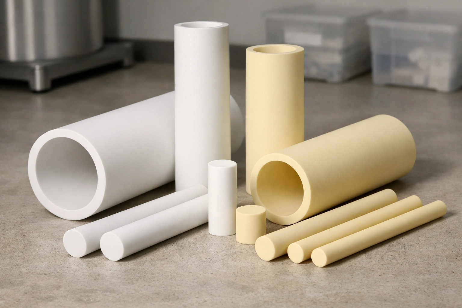
Alumina Plate is commonly treated as a generic ceramic slab, yet in power electronics it functions as an active participant in thermal spreading and electrical isolation. Therefore, its role must be described in system terms before any property table can be interpreted.
-
Substrate relationships and naming conventions
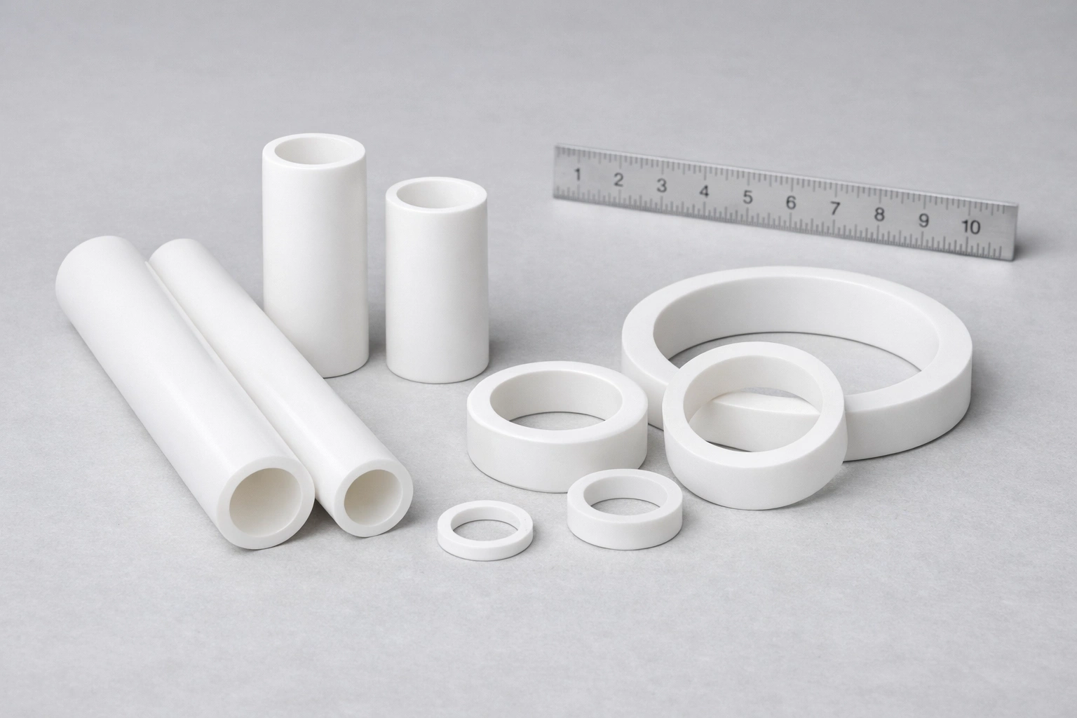
In practice, engineers use Alumina Plate as a precursor to substrates, carriers, insulators, and spacers, depending on how the plate is diced, metallized, or laminated. For instance, thick film circuits often begin with a flat Alumina Plate that later becomes a patterned functional substrate through screen printing and firing. Consequently, identical chemistry can yield different field performance when the downstream process window changes.
Accordingly, the same drawing should state the intended downstream process, because that information determines which surface and flatness metrics are non-negotiable. -
System-level functions inside IGBT and SiC assemblies
In IGBT and SiC stacks, Alumina Plate typically supports two simultaneous functions: it stabilizes the mechanical stack-up and it preserves insulation integrity under high dV/dt stress. Moreover, it often serves as a thermal spreader beneath localized heat sources, even when a separate baseplate handles bulk dissipation. As a result, an Alumina Plate that is “strong enough” can still fail functionally if its interface condition amplifies thermal resistance or concentrates edge fields.
Therefore, engineers should frame selection around the complete heat-flow and field-control chain, not only bulk properties. -
Process coupling with films metallization and attachment layers
During thick film and thin film fabrication, Alumina Plate surface condition directly affects adhesion, trace geometry fidelity, and firing-induced residual stresses. Meanwhile, in LED packaging and automotive modules, attachment layers such as solder, sintered silver, or compliant adhesives can either buffer or magnify the plate’s stiffness and CTE effects. Consequently, a plate that looks stable on incoming inspection may exhibit warp, microcracking, or metallization lift after thermal cycling when the process stack is not co-designed.
Hence, plate specification must be co-authored with process parameters, because process coupling is where many field failures originate.
Summary Criteria for Material Context
| System role focus | What the engineer must clarify | Why it changes the Alumina Plate specification | Typical downstream implication |
|---|---|---|---|
| Thermal spreading | Heat source footprint and heat flux density (W/mm²) | Drives thickness and interface requirements | Junction temperature spread and hotspot suppression |
| Electrical isolation | Operating voltage (V) and dV/dt (kV/µs) | Drives edge geometry and dielectric margins | Partial discharge risk at edges and cutouts |
| Mechanical stack stability | Clamp load (N) and assembly compliance | Drives flatness and fracture margin | Yield loss from chipping, warp, or latent cracks |
| Process compatibility | Film type and firing profile (°C) | Drives surface roughness and residual stress control | Metallization adhesion and dimensional stability |
| Qualification pathway | Thermal cycles (cycles) and ΔT (°C) | Drives microdefect tolerance and inspection strategy | Early-life failures versus wear-out behavior |
Compositional Grades and Microstructural Characteristics
Once the system role of an Alumina Plate is established, engineers inevitably turn to composition and microstructure, because these factors quietly control long-term stability under thermal, electrical, and mechanical coupling.
In power electronic assemblies, differences that appear minor at the datasheet level often manifest as measurable drift after hundreds or thousands of thermal cycles. Therefore, understanding compositional grades and microstructural behavior is foundational before discussing thermal or electrical performance in isolation.
Alumina Purity Levels and Phase Composition
Initially, alumina purity is commonly expressed as a percentage; however, its engineering meaning lies in how secondary phases distribute at grain boundaries. Typical electronic-grade Alumina Plate compositions range from 95% to 99.6% Al₂O₃, with the remaining fraction forming glassy or mixed oxide phases that influence creep, dielectric loss, and thermal stability.
In production environments, 95–96% alumina plates often contain higher silica-based glass phases, which facilitate sintering at lower temperatures around 1550–1600 °C. Consequently, these plates exhibit improved machinability and cost efficiency, yet their grain boundaries soften earlier during prolonged exposure above 300–400 °C. By contrast, 99% and 99.6% grades reduce glass-phase volume significantly, shifting grain-boundary behavior toward crystalline dominance and improving high-temperature stability.
From experience in inverter module platforms, engineers frequently observe that lower-purity Alumina Plate maintains acceptable performance during initial qualification but shows subtle warpage growth after 500–800 thermal cycles. Therefore, purity selection should reflect not only nominal operating temperature but also cumulative thermal exposure across product lifetime.
Grain Structure Density and Defect Population
Beyond purity, grain size distribution and bulk density directly affect fracture behavior and insulation reliability. Fully dense electronic-grade Alumina Plate typically achieves relative densities above 3.85 g/cm³, while grain sizes range from 2 to 6 µm depending on sintering profile.
In practice, finer and more uniform grains reduce stress concentration at triple points, delaying crack initiation under cyclic bending or thermal mismatch. Conversely, plates with bimodal grain distributions often exhibit microcrack nucleation near oversized grains, especially around drilled holes or laser-cut edges. During LED substrate trials, engineers have reported higher chipping rates when average grain size exceeded 7 µm, despite identical nominal flexural strength.
Moreover, residual closed porosity below 1.0% by volume is critical for dielectric stability. Even when bulk breakdown strength exceeds 12–15 kV/mm, localized pores can distort electric fields and accelerate partial discharge inception. Accordingly, microstructural inspection methods such as SEM cross-sections or density mapping become essential when Alumina Plate is used in high-voltage or fast-switching SiC environments.
Microstructural Stability Under Thermal Cycling
Subsequently, microstructure must remain stable under repetitive thermal loading rather than static conditions. Alumina Plate in power modules routinely experiences temperature swings of ΔT = 80–120 °C per cycle, with cumulative cycles exceeding 1000–3000 in automotive duty profiles.
At these conditions, glassy grain-boundary phases can undergo viscous flow, gradually redistributing stress and altering flatness. In contrast, high-purity alumina plates show limited grain-boundary mobility, maintaining dimensional stability but becoming more sensitive to stress concentration if assembly compliance is insufficient. Field-return analyses often reveal that plates failing after extended cycling do not fracture catastrophically; instead, they accumulate microcracks that propagate slowly from edges or metallized interfaces.
Therefore, engineers should interpret microstructural stability as a balance between boundary rigidity and stress accommodation. Selecting an Alumina Plate without considering its grain-boundary response under cyclic thermal stress often leads to late-stage reliability surprises.
Summary of Composition and Microstructure Parameters
| Parameter | Typical Range | Engineering Relevance | Impact on Reliability |
|---|---|---|---|
| Alumina purity (%) | 95–99.6 | Controls glass-phase volume | Thermal stability and creep resistance |
| Bulk density (g/cm³) | 3.7–3.9 | Indicates sintering completeness | Dielectric uniformity and strength |
| Average grain size (µm) | 2–6 | Influences crack initiation | Edge chipping and fatigue life |
| Residual porosity (%) | <1.0 | Affects electric field uniformity | Partial discharge resistance |
| Stable thermal cycles (cycles) | 500–3000 | Reflects microstructural endurance | Long-term dimensional stability |
Thermal Transport Behavior in Power Applications
After compositional stability is clarified, thermal transport becomes the decisive factor for Alumina Plate performance in power electronic assemblies, because temperature gradients directly accelerate electrical and mechanical degradation.
In IGBT modules1, SiC devices, inverters, and LED platforms2, Alumina Plate rarely acts as a primary heat sink. Instead, it governs lateral heat spreading and interface temperature uniformity, which ultimately shapes junction stability and lifetime.
Thermal Conductivity of Alumina Plate Across Grades
First, the thermal conductivity of Alumina Plate varies measurably with purity and microstructure. Electronic-grade alumina typically exhibits thermal conductivity between 18 and 30 W/m·K at room temperature, with higher-purity grades clustering toward the upper end of this range.
In controlled measurements, 96% alumina plates often stabilize near 20–22 W/m·K, while 99.6% alumina plates reach 26–30 W/m·K when grain-boundary glass phases are minimized. However, this advantage diminishes at elevated temperatures. Above 200 °C, thermal conductivity can decline by 15–25%, which is particularly relevant in automotive inverters operating under sustained load.
From field experience in LED module validation, engineers frequently observe that nominal thermal conductivity differences of 5 W/m·K translate into 2–4 °C junction temperature variation across densely packed emitters. Consequently, grade selection should consider effective operating temperature rather than room-temperature datasheet values alone.
Heat Spreading Versus Heat Dissipation Constraints
Next, it is essential to distinguish heat spreading from heat dissipation. Alumina Plate primarily redistributes localized heat laterally, reducing peak temperature gradients beneath chips or traces. Typical Alumina Plate thickness ranges from 0.38 to 1.5 mm in power electronics, chosen to balance spreading efficiency and mechanical stiffness.
In practice, increasing plate thickness improves lateral heat spreading up to a threshold, beyond which thermal resistance through the thickness dominates. For instance, doubling thickness from 0.63 mm to 1.27 mm may reduce hotspot intensity by 10 merging 10–15%, yet simultaneously increase vertical thermal resistance by 20–30%. Engineers often encounter diminishing returns when thickness exceeds 1.5 mm without corresponding improvements in baseplate coupling.
Therefore, Alumina Plate should be optimized as part of a layered thermal stack. Treating it as an isolated heat sink frequently leads to misinterpretation of temperature rise and underperformance during system testing.
Thermal Resistance Accumulation at Interfaces
Finally, interface thermal resistance often outweighs bulk material limitations. In assembled modules, contact resistance at solder, sintered silver, or adhesive layers can account for 40–60% of total thermal resistance between the device junction and baseplate.
During qualification trials, engineers routinely measure acceptable plate conductivity yet observe unexpected temperature rise due to voiding, surface roughness mismatch, or insufficient wetting at interfaces. Even a surface roughness increase from Ra 0.3 µm to 0.8 µm can elevate interface resistance by 10–20%, negating gains achieved through higher-purity Alumina Plate.
Accordingly, thermal design must evaluate Alumina Plate together with interface preparation and attachment processes. Bulk conductivity improvements alone rarely compensate for poorly managed interfaces.
Summary of Thermal Transport Parameters
| Parameter | Typical Range | Engineering Significance | System-Level Impact |
|---|---|---|---|
| Thermal conductivity (W/m·K) | 18–30 | Governs lateral heat spreading | Hotspot suppression |
| Conductivity drop at 200 °C (%) | 15–25 | Affects sustained-load operation | Junction temperature rise |
| Common plate thickness (mm) | 0.38–1.5 | Balances spreading and stiffness | Thermal resistance tradeoff |
| Interface resistance share (%) | 40–60 | Dominates total heat path | Limits effective cooling |
| Junction temperature variation (°C) | 2–4 | Caused by grade differences | Reliability margin |

Electrical Insulation Performance and Reliability
However, thermal control alone does not guarantee system stability, because Alumina Plate simultaneously carries the burden of electrical insulation under increasingly aggressive voltage and switching conditions.
In IGBT, SiC, automotive, and LED power systems, electrical stress often rises faster than temperature, especially as switching frequencies and edge rates increase. Therefore, insulation reliability must be examined with equal rigor and system awareness.
Dielectric Strength and Breakdown Mechanisms
First, dielectric strength defines the maximum electric field Alumina Plate can withstand before catastrophic failure. Typical dielectric strength for electronic-grade Alumina Plate ranges from 10 to 15 kV/mm, depending on purity, density, and surface condition.
In laboratory tests, breakdown rarely occurs uniformly through the bulk. Instead, it initiates at microstructural weak points such as residual pores, surface scratches, or edge defects. For example, during high-voltage ramp tests on SiC gate driver substrates, engineers often observe breakdown initiating at laser-cut corners rather than flat central regions, even when average field strength remains below 8 kV/mm.
Consequently, dielectric strength should be treated as a statistical property rather than a single guaranteed value. Plate geometry, surface finish, and edge treatment frequently determine real-world insulation margins more than nominal bulk data.
Volume Resistivity and Long-Term Stability
Next, volume resistivity governs leakage behavior under continuous bias. Alumina Plate typically exhibits volume resistivity above 10¹⁴ Ω·cm at room temperature, which ensures minimal leakage in most low- to mid-voltage applications.
Nevertheless, resistivity decreases exponentially with temperature. At 150–200 °C, resistivity may drop by one to two orders of magnitude, particularly in lower-purity grades containing higher glass-phase content. In automotive inverter platforms operating under sustained thermal load, this gradual change can increase leakage currents and local heating, subtly accelerating aging mechanisms.
From long-term endurance testing, engineers have noted that resistivity drift, rather than immediate breakdown, often serves as the earliest indicator of insulation degradation. Therefore, specifying Alumina Plate purely by room-temperature resistivity can mask long-term reliability risks.
Partial Discharge and Edge Field Concentration
Finally, partial discharge behavior increasingly dominates insulation design in fast-switching environments. Modern SiC systems routinely exceed dV/dt levels of 20–50 kV/µs, intensifying electric field concentration at edges, holes, and metallization boundaries.
In practice, partial discharge inception voltage (PDIV) depends strongly on edge geometry and surface condition. A sharp edge with radius below 50 µm can reduce PDIV by 30–40% compared to a properly chamfered or rounded profile. During qualification of automotive power modules, engineers often eliminate early PD failures simply by revising edge finishing specifications rather than changing material grade.
Thus, Alumina Plate insulation reliability emerges from a combination of bulk properties and geometric discipline. Ignoring edge field management frequently leads to unexpected discharge activity despite apparently conservative material choices.
Summary of Electrical Insulation Parameters
| Parameter | Typical Range | Engineering Relevance | Reliability Impact |
|---|---|---|---|
| Dielectric strength (kV/mm) | 10–15 | Sets maximum field margin | Breakdown resistance |
| Volume resistivity (Ω·cm) | ≥10¹⁴ | Controls leakage behavior | Long-term insulation stability |
| Resistivity drop at 200 °C (orders) | 1–2 | Indicates thermal sensitivity | Aging acceleration |
| dV/dt tolerance (kV/µs) | 20–50 | Reflects switching stress | Partial discharge risk |
| Edge radius influence (%) | 30–40 | Alters PD inception voltage | Early-life failures |
Mechanical Integrity Under Assembly and Service Loads
Nevertheless, even when thermal and electrical margins appear sufficient, mechanical integrity often determines whether an Alumina Plate survives real assembly and service conditions without latent damage.
In power modules, inverters, automotive electronics, and LED platforms, mechanical stress rarely appears as a single overload event. Instead, it accumulates gradually through clamping, bonding, vibration, and thermal mismatch, making early-stage design discipline essential.
Flexural Strength and Thickness Dependence
First, flexural strength establishes the baseline load-bearing capacity of an Alumina Plate. Electronic-grade alumina typically exhibits flexural strength between 300 and 450 MPa, depending on purity, grain size, and flaw population.
However, flexural strength scales nonlinearly with thickness. In practice, doubling thickness from 0.63 mm to 1.27 mm can increase bending stiffness by nearly eight times, yet it also amplifies thermal mismatch stress when bonded to metals with higher CTE. During inverter platform development, engineers often find that thin plates fracture during handling, while overly thick plates crack later during thermal cycling.
Accordingly, thickness selection should balance handling robustness against long-term stress accumulation. Treating thickness purely as a safety margin frequently shifts failure from assembly to service life rather than eliminating it.
Residual Stress From Processing and Assembly
Next, residual stress introduced during processing and assembly significantly affects fracture risk. Grinding, lapping, and polishing can introduce subsurface damage layers up to 10–30 µm deep if process parameters are not optimized.
In addition, attachment methods such as soldering or sintered silver bonding impose thermal excursions of 200–300 °C, generating residual stresses that persist after cooling. Engineers have observed that plates passing incoming inspection often crack only after bonding, when tensile stress concentrates near corners or holes. Even compliant adhesive layers can transmit sufficient stress to initiate microcracks if thickness uniformity varies by more than ±10%.
Therefore, mechanical integrity cannot be assessed solely on incoming plate condition. It must be evaluated after the full assembly process, because residual stress states evolve throughout manufacturing.
Fracture Initiation in Real Assemblies
Finally, fracture initiation typically occurs at predictable but often overlooked locations. Edges, drilled holes, laser-cut features, and metallization boundaries serve as stress concentrators under combined mechanical and thermal loading.
Field-return analyses from automotive electronics frequently show crack origins within 0.2–0.5 mm of an edge or hole, even when bulk stress calculations suggest ample margin. These cracks propagate slowly under cyclic loading, remaining undetected until catastrophic separation occurs after hundreds of cycles.
Thus, mechanical reliability hinges on disciplined geometric detailing and stress-aware assembly design. Ignoring fracture initiation sites commonly results in delayed failures that evade early qualification screens.
Summary of Mechanical Integrity Parameters
| Parameter | Typical Range | Engineering Significance | Failure Implication |
|---|---|---|---|
| Flexural strength (MPa) | 300–450 | Baseline load capacity | Handling and assembly robustness |
| Subsurface damage depth (µm) | 10–30 | Result of machining | Crack initiation risk |
| Bonding thermal excursion (°C) | 200–300 | Induces residual stress | Post-assembly cracking |
| Edge crack origin distance (mm) | 0.2–0.5 | Common failure initiation zone | Latent service failures |
| Thickness variation tolerance (%) | ±10 | Stress uniformity control | Bond-line stress amplification |

Surface Condition and Secondary Processing Compatibility
Meanwhile, once bulk mechanical integrity is secured, surface condition becomes the decisive interface between Alumina Plate and downstream electronic processes, because surfaces govern adhesion, stress transfer, and dimensional fidelity.
In thick film, thin film, LED, and power module fabrication, surface-related issues rarely cause immediate failure. Instead, they degrade yield gradually, making surface control a silent determinant of long-term stability.
Surface Roughness and Film Adhesion
Initially, surface roughness directly affects metallization and dielectric film adhesion. Typical Alumina Plate surface roughness for electronic applications ranges from Ra 0.2 to 0.8 µm, depending on whether lapped or polished finishes are applied.
In thick film circuits, moderately rough surfaces around Ra 0.4–0.6 µm promote mechanical interlocking of conductive pastes during firing. Conversely, thin film and sputtered metallization processes often require smoother surfaces below Ra 0.3 µm to ensure uniform film thickness and minimize pinhole formation. Engineers transitioning between these processes frequently encounter adhesion loss when surface finish is not re-specified accordingly.
From production experience, adhesion failures commonly appear after 200–400 thermal cycles, not during initial pull tests. Therefore, roughness selection should reflect service conditions rather than only initial adhesion metrics.
Lapping Polishing and Dimensional Stability
Next, lapping and polishing influence both surface quality and residual stress. Lapped Alumina Plate surfaces typically maintain better thickness uniformity across large areas, while polished surfaces achieve lower roughness at the expense of higher subsurface stress if parameters are aggressive.
In inverter module platforms, engineers have observed that aggressive polishing can introduce tensile surface layers leading to microcrack formation after bonding. Measurements often reveal flatness deviations increasing from ≤20 µm to ≥50 µm after thermal cycling, despite meeting incoming flatness specifications. By contrast, controlled lapping with conservative removal rates tends to preserve dimensional stability under repeated heating.
Thus, surface finish must be specified alongside acceptable material removal depth and process discipline, because finish alone does not guarantee stability.
Laser Machining Drilling and Edge Quality
Finally, secondary machining such as laser cutting and drilling introduces localized thermal damage that can undermine otherwise robust Alumina Plate performance. Laser-affected zones typically extend 30–80 µm from cut edges, depending on pulse energy and repetition rate.
In real assemblies, these zones act as preferred crack initiation sites under combined thermal and mechanical stress. Engineers validating SiC gate driver substrates often report higher early-life failure rates when laser-cut edges are left untreated. Simple post-processing steps such as edge grinding or controlled chamfering can reduce crack initiation frequency by 40–60%, even without changing material grade.
Accordingly, secondary processing compatibility should be evaluated as part of the Alumina Plate specification, not delegated entirely to downstream fabrication.
Summary of Surface and Processing Parameters
| Parameter | Typical Range | Engineering Relevance | Reliability Outcome |
|---|---|---|---|
| Surface roughness Ra (µm) | 0.2–0.8 | Film adhesion control | Metallization stability |
| Thin film target Ra (µm) | ≤0.3 | Thickness uniformity | Reduced pinholes |
| Subsurface stress depth (µm) | 10–30 | From polishing | Thermal cycle deformation |
| Laser heat-affected zone (µm) | 30–80 | Edge damage extent | Crack initiation risk |
| Edge treatment benefit (%) | 40–60 | Failure reduction | Improved service life |
Dimensional Control and Geometric Design Considerations
Subsequently, after surface condition and secondary processing are stabilized, dimensional control emerges as a system-level constraint, because geometry governs how thermal, electrical, and mechanical stresses distribute throughout the Alumina Plate.
In power electronics and film-based circuit platforms, dimensional deviations rarely appear dramatic at inspection. Nevertheless, even small geometric inconsistencies can cascade into yield loss and long-term reliability drift once assemblies enter cyclic service.
Flatness Warpage and Assembly Yield
First, flatness directly influences assembly yield and interface reliability. Typical flatness requirements for Alumina Plate in power modules range from 10 to 50 µm across the full plate area, depending on attachment method and footprint size.
In practical inverter module builds, plates exceeding 40 µm flatness deviation often exhibit uneven bond-line thickness, which concentrates stress during thermal cycling. Engineers frequently report that such plates pass initial bonding yet develop localized delamination after 300–600 cycles, particularly near corners where constraint is highest.
Accordingly, flatness must be specified relative to both plate size and bonding compliance. Treating flatness as a generic tolerance without considering assembly mechanics often results in false acceptance during incoming inspection.
Hole Slot and Cutout Design Limits
Next, holes, slots, and cutouts introduce unavoidable stress concentrators. Minimum edge-to-hole distances of 1.5–2.0 times the plate thickness are commonly required to maintain fracture resistance under combined load.
In real assemblies, engineers validating gate driver substrates have observed crack initiation when slot widths fall below 0.8 mm in plates thinner than 0.63 mm, even though bulk strength calculations suggested adequacy. Laser-cut features with sharp internal corners further amplify stress, reducing fracture margin during thermal excursions.
Therefore, geometric features should be designed with stress redistribution in mind. Rounded corners, generous fillets, and conservative feature spacing often improve reliability more effectively than increasing material grade.
Size Scaling Effects on Reliability
Finally, scaling plate dimensions introduces non-linear reliability effects. As plate length or width increases, thermal expansion mismatch forces scale with area, while bending stiffness scales differently with thickness.
In large-format LED boards and inverter substrates exceeding 150 mm in length, engineers frequently encounter warpage growth beyond 2–3 times that observed in smaller samples during thermal cycling. These effects are rarely predicted by small-sample testing, leading to unexpected failures late in development.
Thus, dimensional scaling should be treated as a distinct design variable. Validation data from small coupons cannot be directly extrapolated to full-size Alumina Plate implementations without additional safety margin.
Summary of Dimensional and Geometric Parameters
| Parameter | Typical Range | Engineering Significance | Impact on Yield |
|---|---|---|---|
| Flatness tolerance (µm) | 10–50 | Bond-line uniformity | Assembly consistency |
| Critical flatness threshold (µm) | ≥40 | Stress concentration onset | Delamination risk |
| Edge-to-hole ratio | 1.5–2.0 × thickness | Fracture resistance | Crack prevention |
| Slot width in thin plates (mm) | ≥0.8 | Feature integrity | Reduced edge failure |
| Large-format warpage increase | 2–3 × | Size scaling effect | Late-stage failures |

Alumina Plate Versus Alternative Ceramic Substrates
Conversely, once dimensional stability is addressed, material selection inevitably broadens to comparisons with alternative ceramic substrates, because engineers must justify why Alumina Plate remains appropriate amid expanding material options.
In power electronic systems, such comparisons are rarely academic. Instead, they reflect tradeoffs among thermal performance, mechanical reliability, manufacturability, supply continuity, and qualification risk across product lifecycles.
Alumina and Aluminum Nitride Tradeoffs
First, aluminum nitride is frequently proposed as a thermal upgrade due to its higher thermal conductivity. Aluminum nitride substrates typically exhibit thermal conductivity between 140 and 180 W/m·K, compared to 18–30 W/m·K for Alumina Plate.
However, this thermal advantage introduces secondary constraints. Aluminum nitride is more sensitive to moisture ingress, requiring controlled storage and handling. Moreover, its lower fracture toughness and higher cost often limit its use to applications where junction temperature margins are already exhausted. In inverter programs evaluated for both materials, engineers commonly find that switching to aluminum nitride reduces junction temperature by 5–10 °C, yet increases procurement lead time and fracture-related yield loss.
Therefore, Alumina Plate remains favored when thermal demands can be satisfied through stack optimization rather than material substitution, preserving mechanical robustness and supply stability.
Alumina and Silicon Nitride in Power Modules
Next, silicon nitride enters consideration due to its superior fracture toughness and fatigue resistance. Silicon nitride substrates typically achieve fracture toughness values above 6 MPa·m¹ᐟ², compared to 3–4 MPa·m¹ᐟ² for alumina.
In high-vibration or high-shock environments, such as traction inverters, silicon nitride can significantly improve mechanical survival. Nevertheless, its thermal conductivity, typically 70–90 W/m·K, still trails aluminum nitride, and its processing routes limit available thicknesses and geometries. Engineers often report that silicon nitride substrates perform exceptionally well in mechanically demanding platforms but impose constraints on metallization and attachment processes.
Consequently, Alumina Plate continues to dominate applications where mechanical shock is moderate and where compatibility with established thick film or DBC processes is essential.
Why Alumina Remains Widely Adopted
Finally, Alumina Plate persists as a widely adopted substrate because it occupies a balanced position across competing requirements. Its combination of moderate thermal conductivity, high dielectric strength, predictable fracture behavior, and broad manufacturing maturity enables stable design reuse across product generations.
From program retrospectives, engineers frequently conclude that while alternative ceramics solve specific bottlenecks, they also introduce new risks that complicate qualification. Alumina Plate, by contrast, allows incremental optimization through geometry, surface condition, and interface engineering rather than wholesale material changes.
Thus, material selection should reflect system-level optimization rather than isolated parameter maximization. Alumina Plate remains relevant not by excelling in a single metric, but by minimizing total program risk.
Summary of Ceramic Substrate Comparisons
| Material | Thermal Conductivity (W/m·K) | Fracture Toughness (MPa·m¹ᐟ²) | Key Advantage | Key Constraint |
|---|---|---|---|---|
| Alumina Plate | 18–30 | 3–4 | Balanced performance and maturity | Moderate thermal conductivity |
| Aluminum Nitride | 140–180 | 2–3 | Superior heat conduction | Moisture sensitivity and cost |
| Silicon Nitride | 70–90 | ≥6 | High mechanical robustness | Process and geometry limits |
| Zirconia-based | 2–3 | ≥7 | Extreme toughness | Poor thermal transport |
Failure Modes Observed in Electronic Applications
Nevertheless, even when Alumina Plate is selected with sound material reasoning, failures still emerge in electronic applications, because real operating conditions combine thermal, electrical, and mechanical stresses in ways that exceed simplified assumptions.
In power modules, inverters, automotive electronics, LED platforms, and film circuits, failure analysis repeatedly shows that Alumina Plate rarely fails randomly. Instead, failures follow recognizable patterns that can be anticipated and mitigated through informed design.
Thermo-Mechanical Cracking Scenarios
First, thermo-mechanical cracking represents the most common long-term failure mode. Repeated thermal cycling with ΔT values between 80 and 120 °C generates cyclic tensile and compressive stresses driven by CTE mismatch between Alumina Plate and bonded metals.
In practice, cracks typically initiate at geometric discontinuities such as corners, holes, or metallization edges. Engineers reviewing returned inverter modules often identify crack origins within 0.3 mm of a corner, where stress concentration amplifies local strain. These cracks may propagate slowly over 500–1500 cycles, remaining electrically silent until sudden fracture causes functional loss.
Therefore, thermo-mechanical cracking should be treated as a cumulative damage process. Designs that appear stable in early qualification can still fail later if stress amplitude and cycle count are underestimated.
Electrical Degradation and Surface Tracking
Next, electrical degradation manifests through surface tracking and insulation weakening rather than immediate breakdown. Sustained electric fields above 5–7 kV/mm, especially in humid or contaminated environments, can initiate surface conduction paths.
In field observations from LED driver boards and automotive control units, engineers have documented gradual discoloration and micro-arcing along alumina surfaces adjacent to metallized traces. These effects often emerge after 1000–2000 operating hours, coinciding with increased leakage currents rather than abrupt failure.
Accordingly, electrical degradation should be monitored as a progressive phenomenon. Surface finish, cleanliness, and edge geometry play decisive roles in delaying tracking onset.
Interface Delamination and Bond Failure
Finally, interface-related failures frequently dominate system-level reliability outcomes. Bond layers between Alumina Plate and metals or substrates account for a significant portion of thermal and mechanical compliance, making them vulnerable to fatigue.
During accelerated life testing, engineers commonly observe delamination initiating at bond-line voids exceeding 5–10% area fraction, even when bulk material properties meet specification. These delaminations reduce heat transfer efficiency and increase local stress, accelerating subsequent cracking.
Thus, failure prevention must extend beyond Alumina Plate itself. Interface quality, bonding uniformity, and attachment process control are integral components of reliability engineering.
Summary of Common Failure Modes
| Failure Mode | Typical Trigger | Observed Threshold | Reliability Consequence |
|---|---|---|---|
| Thermo-mechanical cracking | Thermal cycling | ΔT 80–120 °C | Delayed fracture |
| Surface tracking | High electric field | 5–7 kV/mm | Leakage and insulation loss |
| Interface delamination | Bond-line defects | 5–10% void area | Thermal resistance rise |
| Edge-initiated fracture | Geometric stress | <0.3 mm from edge | Sudden failure |
| Progressive leakage | Long-term bias | 1000–2000 hours | Early performance drift |

Application-Specific Considerations
Moreover, after understanding generic failure mechanisms, engineers must contextualize Alumina Plate behavior within specific electronic architectures, because each application imposes distinct thermal, electrical, and mechanical constraints.
Although the same Alumina Plate chemistry may be used across platforms, its effective reliability depends on how it is integrated, loaded, and cycled in each system topology.
IGBT and SiC Power Module Architectures
First, IGBT and SiC power modules place Alumina Plate at the intersection of high heat flux and fast electrical switching. Typical heat flux densities range from 50 to 200 W/cm², while dV/dt values in SiC modules frequently exceed 30 kV/µs.
In practical module stacks, Alumina Plate often sits beneath metallized layers and above baseplates or heat spreaders. Engineers consistently observe that plates thinner than 0.63 mm struggle to distribute localized heat from high-current traces, while plates thicker than 1.27 mm introduce excessive through-thickness thermal resistance. During qualification of traction inverters, optimal performance commonly appears in the 0.63–1.0 mm thickness window, balancing lateral spreading and vertical conduction.
Therefore, Alumina Plate in power modules must be specified with explicit reference to switching speed, chip density, and attachment method. Treating it as a generic insulator frequently leads to underestimating coupled thermal-electrical stress.
Inverters and Automotive Electronics
Next, automotive electronics impose long-duration reliability requirements under combined thermal cycling and vibration. Automotive inverter platforms typically experience 1000–3000 thermal cycles over service life, with ambient temperatures ranging from −40 to 125 °C.
In these systems, Alumina Plate must tolerate not only thermal mismatch but also mechanical excitation. Engineers evaluating field returns often find microcracks aligned with vibration modes rather than purely thermal gradients. Plates with insufficient edge finishing or inconsistent flatness amplify these effects, leading to early fatigue.
Accordingly, automotive applications favor conservative geometry, generous edge radii, and stable microstructures over marginal thermal gains. Alumina Plate selection here prioritizes endurance and predictability rather than peak performance metrics.
LED Packaging and Thermal Platforms
Subsequently, LED packaging emphasizes temperature uniformity across arrays rather than extreme heat flux at a single point. LED junction temperature variation of just 3–5 °C can produce visible brightness non-uniformity and accelerated lumen depreciation.
In LED boards, Alumina Plate often functions as a thermal equalizer beneath multiple emitters. Engineers routinely report that surface flatness deviations above 30 µm lead to uneven solder thickness and localized overheating. Moreover, surface roughness incompatible with solder or adhesive layers can trap voids, increasing thermal resistance by 15–25%.
Thus, in LED systems, Alumina Plate performance is judged by uniformity and consistency rather than maximum conductivity. Small geometric and surface deviations often outweigh material-grade differences.
Thick Film and Thin Film Circuit Systems
Finally, thick film and thin film circuit systems place unique demands on Alumina Plate due to repeated firing or deposition processes. Thick film firing cycles commonly reach 850–900 °C, while thin film deposition involves precise surface energy control.
In thick film circuits, plates must resist warpage during multiple firing cycles without accumulating residual stress. Engineers often observe that plates with uneven grain structure warp progressively after 3–5 firing cycles, even if initial flatness meets specification. Thin film systems, by contrast, are more sensitive to surface roughness and contamination, with defect density rising sharply when Ra exceeds 0.3 µm.
Consequently, circuit-oriented applications require Alumina Plate specifications tightly coupled to process parameters. Decoupling material selection from fabrication sequence frequently leads to yield erosion.
Summary of Application-Specific Requirements
| Application | Dominant Stress | Typical Threshold | Alumina Plate Priority |
|---|---|---|---|
| IGBT and SiC modules | Heat flux and dV/dt | 50–200 W/cm²; >30 kV/µs | Balanced thickness and edge control |
| Automotive inverters | Thermal cycling and vibration | 1000–3000 cycles | Endurance and geometry stability |
| LED packaging | Temperature uniformity | ΔT 3–5 °C | Flatness and surface consistency |
| Thick film circuits | Repeated high-temperature firing | 850–900 °C cycles | Warpage resistance |
| Thin film circuits | Surface energy and cleanliness | Ra ≤0.3 µm | Surface quality and uniformity |
Specification Development for Engineering Drawings
Subsequently, once application boundaries are clear, Alumina Plate performance depends heavily on how engineering intent is translated into drawings, because specifications govern what is actually manufactured, inspected, and delivered.
In power electronic programs, many downstream failures trace back to ambiguous or misprioritized drawing requirements rather than material limitations. Therefore, specification development must reflect functional risk rather than generic completeness.
Core Parameters Commonly Required
Initially, drawings for Alumina Plate typically list material grade, dimensions, and surface condition; however, only a subset of parameters consistently controls reliability. Thickness, flatness, surface roughness, and edge condition usually dominate performance outcomes across power modules, LED boards, and film circuits.
From experience supporting inverter and gate driver platforms, engineers often discover that over-specified minor dimensions coexist with under-specified critical interfaces. For instance, drawings may tightly control overall length to ±0.05 mm while leaving flatness undefined, despite flatness directly affecting bond-line uniformity and thermal stress. As a result, inspection passes yet assembly yield suffers.
Accordingly, core parameters should be elevated to primary callouts with explicit limits, while secondary dimensions receive pragmatic tolerances aligned with manufacturing capability.
Tolerances That Actually Matter
Next, tolerance selection must correspond to stress sensitivity rather than nominal geometry. Flatness tolerances between 15 and 40 µm commonly represent the threshold at which bonding uniformity and crack risk change significantly, depending on plate size and attachment method.
In automotive inverter programs, engineers have observed that tightening flatness from 40 µm to 25 µm reduces post-cycling delamination incidents by more than 30%, even when all other parameters remain constant. Conversely, tightening non-critical hole position tolerances often increases cost without measurable reliability gain.
Therefore, tolerances should be distributed strategically. Emphasizing stress-critical features improves system robustness more effectively than uniformly tightening all dimensions.
Avoiding Over-Specification Risks
Finally, over-specification introduces hidden reliability and supply risks. Excessively tight tolerances can force aggressive grinding or polishing, increasing subsurface damage depth beyond 20–30 µm and raising crack initiation probability.
In practice, engineers sometimes specify surface roughness below Ra 0.2 µm for thick film applications, assuming smoother is always better. However, this level of finish can reduce metallization adhesion and amplify residual stress, leading to failures after 200–500 thermal cycles. Such outcomes illustrate that tighter specifications are not inherently safer.
Thus, specification development should balance functional necessity with process realism. Drawings that reflect real stress drivers consistently outperform those optimized for nominal precision alone.
Summary of Drawing Specification Priorities
| Specification Item | Typical Effective Range | Engineering Rationale | Reliability Effect |
|---|---|---|---|
| Plate thickness (mm) | 0.38–1.5 | Balances stiffness and thermal resistance | Stress and heat spreading control |
| Flatness (µm) | 15–40 | Governs bond-line uniformity | Delamination reduction |
| Surface roughness Ra (µm) | 0.3–0.8 | Adhesion and stress balance | Stable metallization |
| Edge condition radius (µm) | ≥50 | Field and stress mitigation | Crack and PD suppression |
| Dimensional tolerances (mm) | Application-specific | Manufacturability alignment | Cost and yield stability |
Qualification and Validation Approaches
Meanwhile, after specifications are finalized, qualification and validation establish whether an Alumina Plate can sustain real operating conditions rather than only satisfying incoming inspection criteria.
In power electronic systems, validation failures rarely stem from missing tests; instead, they arise when tests are disconnected from actual stress profiles encountered during service.
-
Sample-level screening and baseline verification
Early qualification typically begins with dimensional inspection, density checks, and dielectric testing to confirm compliance with drawings. However, these steps only verify manufacturing consistency, not functional endurance. For example, plates that pass dielectric testing at 12 kV/mm may still exhibit partial discharge activity once assembled into fast-switching SiC environments.
Therefore, baseline screening should be treated as a gate, not a guarantee, and followed by stress-relevant validation. -
Assembly-integrated thermal and electrical cycling
Meaningful validation requires testing Alumina Plate within representative assemblies rather than as isolated coupons. Thermal cycling between −40 and 125 °C or −40 and 150 °C for 500–3000 cycles reveals warpage growth, interface degradation, and latent cracking that coupon tests cannot capture. Similarly, electrical endurance under realistic bias and switching conditions exposes leakage drift before catastrophic failure.
Consequently, validation protocols should replicate assembly constraints, attachment methods, and load paths. -
Correlation between accelerated tests and field behavior
Accelerated tests are effective only when their stress modes align with field usage. Engineers frequently encounter cases where aggressive temperature ramps induce failures that never appear in service, while moderate but long-duration cycling reveals progressive degradation.
Thus, validation should emphasize stress similarity rather than test severity, ensuring that observed failure modes correspond to real-world risks.
In summary, qualification and validation succeed when they reflect how Alumina Plate actually functions inside power electronic systems, closing the gap between laboratory compliance and field reliability.
Summary of Qualification and Validation Parameters
| Validation Aspect | Typical Condition | Engineering Purpose | Reliability Insight |
|---|---|---|---|
| Incoming screening | Density and dielectric checks | Manufacturing consistency | Defect filtering |
| Thermal cycling | −40 to 125 °C, 500–3000 cycles | Stress endurance | Crack and delamination onset |
| Electrical endurance | Sustained bias and switching | Insulation stability | Leakage and PD trends |
| Assembly-level testing | Representative stack-up | Interface realism | System-level failure modes |
| Correlation analysis | Test vs field data | Risk prediction accuracy | Validation effectiveness |

Customization Strategy for System-Level Optimization
Moreover, once qualification data exposes system sensitivities, customization becomes a practical extension of engineering control rather than a deviation from standard practice.
In power electronic assemblies, Alumina Plate customization is most effective when it targets stress redistribution, interface stability, and process compatibility simultaneously. Consequently, customization should be framed as system optimization, not cosmetic variation.
When Standard Alumina Plates Become Insufficient
Initially, standard Alumina Plate formats satisfy many applications; however, limitations surface as power density, switching speed, and package integration increase. Programs exceeding heat flux levels of 120–150 W/cm² or experiencing thermal cycles beyond 1500 cycles often reveal constraints that standard dimensions cannot mitigate.
In real inverter and SiC gate driver projects, engineers commonly encounter edge cracking or localized delamination despite compliant material grades. These issues persist because standard geometries fail to redistribute stress away from corners, holes, or bonded interfaces. For instance, a standard rectangular plate may concentrate stress at sharp internal cutouts, triggering cracks after 600–900 cycles.
Therefore, recognizing the transition point where standard formats lose margin is essential. Customization should be triggered by observed stress localization rather than by arbitrary performance targets.
Geometry Thickness and Surface Customization
Next, geometry and surface customization offer the highest return on reliability improvement. Incremental thickness adjustments of 0.2–0.4 mm can shift bending stiffness enough to reduce peak tensile stress by 20–35%, particularly near bonded interfaces.
Similarly, tailored surface finishes aligned with attachment methods stabilize interfaces. In sintered silver bonding, engineers often specify surface roughness within Ra 0.3–0.5 µm, while solder-based systems tolerate Ra up to 0.8 µm without void proliferation. Field experience shows that aligning surface finish to bonding chemistry reduces void growth rates by 25–40% during thermal cycling.
Thus, customization should prioritize dimensions and surfaces that directly influence stress and heat flow. Broad changes to material grade alone rarely deliver comparable gains.
Engineering Feedback Loops
Finally, effective customization depends on feedback loops between design, manufacturing, and validation. Iterative adjustment cycles typically span 2–4 design revisions, each informed by warpage measurements, crack mapping, and thermal data.
In practice, engineering teams that share assembly data with material suppliers converge on stable configurations faster than those operating in isolation. For example, revising edge radii from 30 µm to 80 µm based on fracture mapping can reduce early-life failures by more than 50% without altering the core material.
Accordingly, customization should be treated as a collaborative process anchored in measurement and iteration. Closed-loop feedback transforms Alumina Plate from a fixed component into a tunable system element.
Summary of Customization Levers and Effects
| Customization Lever | Typical Adjustment | Engineering Benefit | Reliability Outcome |
|---|---|---|---|
| Thickness tuning (mm) | +0.2 to +0.4 | Stress redistribution | Crack reduction |
| Edge radius (µm) | 50–100 | Field and stress mitigation | Lower PD and fracture risk |
| Surface roughness Ra (µm) | 0.3–0.8 | Interface compatibility | Stable bonding |
| Geometry tailoring | Fillets and cutouts | Stress homogenization | Extended cycle life |
| Iteration cycles (count) | 2–4 | Data-driven refinement | Faster convergence |
Engineering Collaboration With ADCERAX
Moreover, once system-level customization becomes necessary, outcomes increasingly depend on how effectively material suppliers integrate into the engineering workflow rather than on material specifications alone.
ADCERAX approaches Alumina Plate supply as an engineering collaboration, aligning material selection, geometry control, and process feedback with real application constraints in power electronic systems.
ADCERAX supports customization starting from customer drawings and application descriptions, then provides targeted engineering recommendations on thickness windows, flatness limits, surface finish, and edge treatment based on stress distribution and thermal paths. Furthermore, small-batch prototyping enables early validation under representative assembly conditions before committing to volume production. Additionally, in-stock standard Alumina Plate formats allow rapid iteration cycles, while controlled process routes ensure consistency once designs are frozen.
Consequently, ADCERAX functions as a technical extension of the customer’s engineering team, helping reduce late-stage redesigns and accelerating convergence toward stable, production-ready Alumina Plate solutions.
Closing Perspective on Alumina Plate Selection
Ultimately, Alumina Plate remains a cornerstone material in power electronic systems because its performance emerges from balanced engineering rather than extreme properties.
When composition, geometry, surface condition, and interfaces are considered together, Alumina Plate delivers predictable thermal spreading, reliable insulation, and mechanical stability across demanding applications. Accordingly, disciplined selection and collaborative optimization continue to outperform isolated material substitutions as power density and system complexity increase.
Conclusion
In essence, Alumina Plate reliability in power electronics depends on integrated decisions spanning material, geometry, processing, and validation rather than any single parameter.
For engineers seeking application-specific Alumina Plate solutions, ADCERAX offers engineering-driven customization and rapid validation support aligned with real power electronic system demands.
FAQ
What Alumina Plate thickness is commonly used in power modules
Most IGBT and SiC power modules use Alumina Plate thicknesses between 0.63 and 1.0 mm, balancing heat spreading and mechanical stability.
Is higher purity Alumina Plate always better for electronics
Not necessarily. Higher purity improves thermal and electrical stability, but lower-purity grades may perform adequately when geometry and interfaces are properly optimized.
How does surface finish affect long-term reliability
Surface roughness influences bonding quality and residual stress. Mismatched finishes can cause void growth and delamination after hundreds of thermal cycles.
When should customization replace standard Alumina Plate formats
Customization becomes necessary when standard plates show stress localization, warpage growth, or interface degradation during validation or extended thermal cycling.
References: