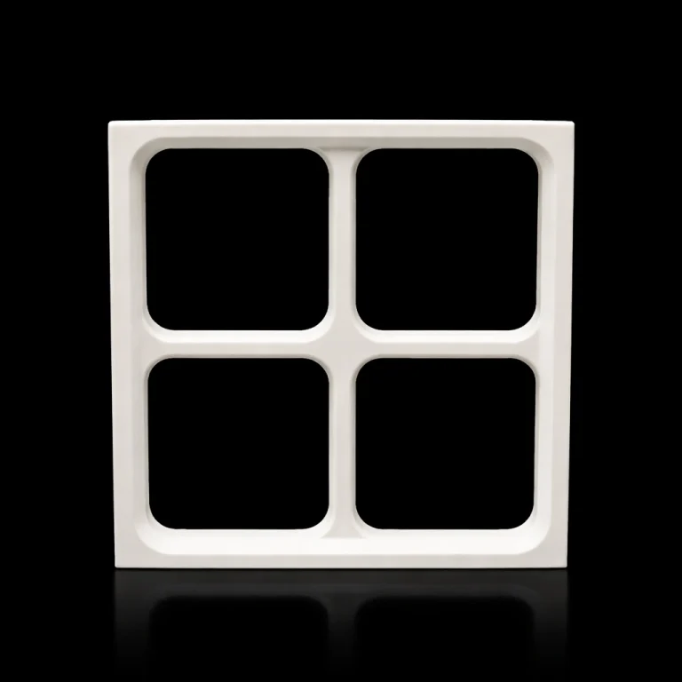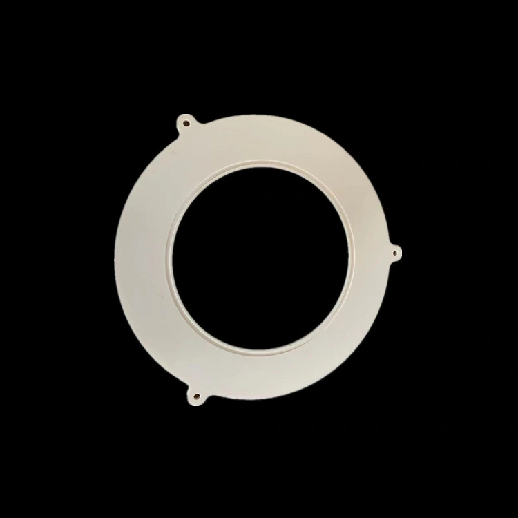
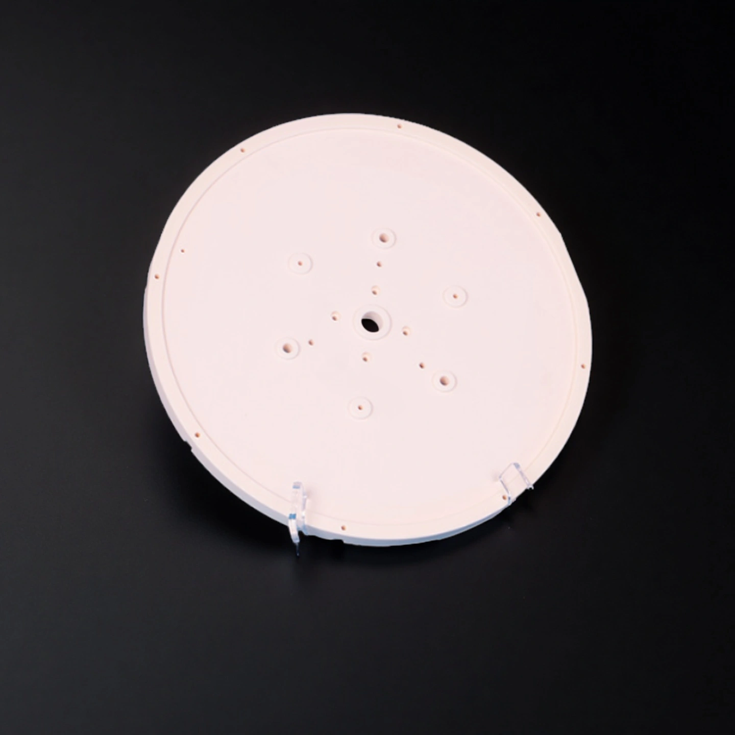
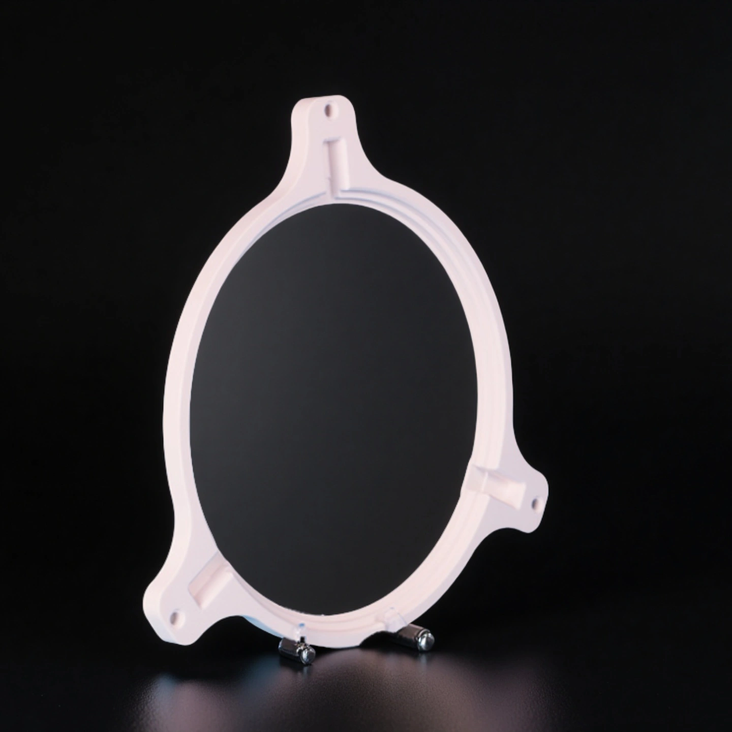
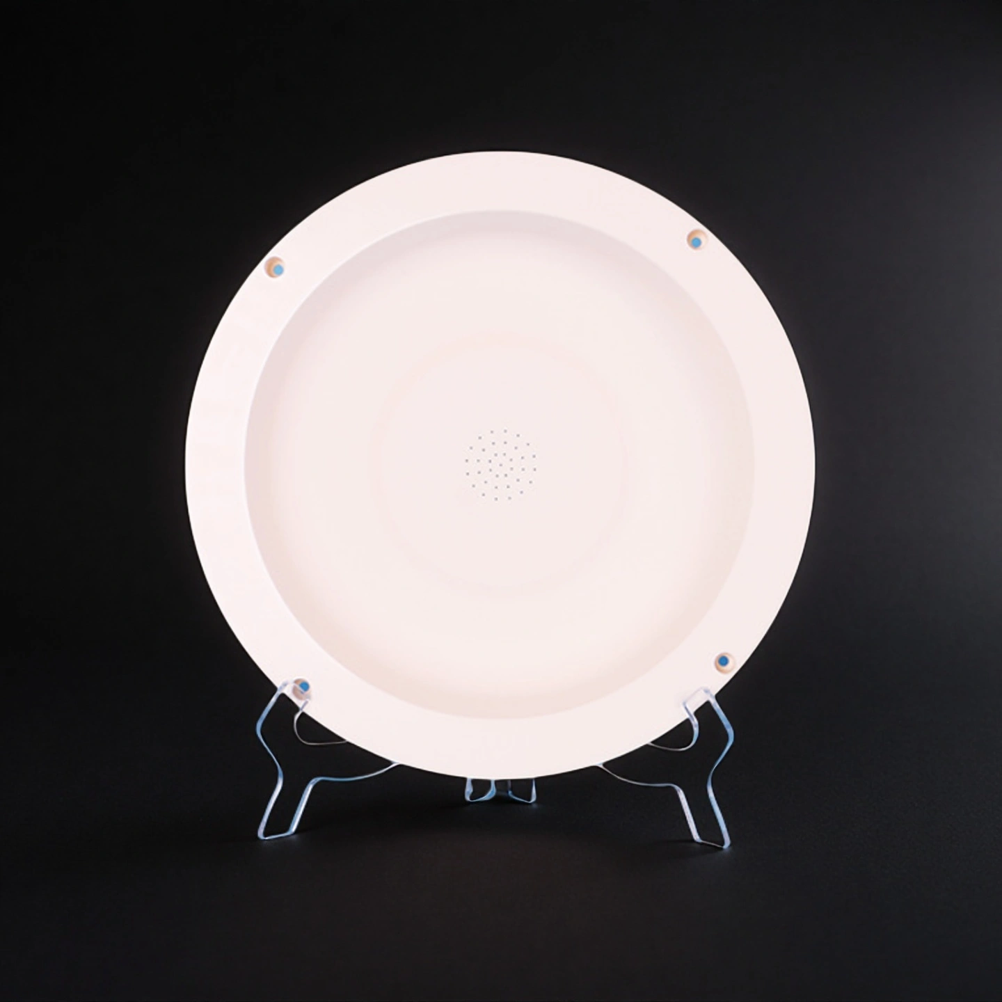
Alumina semiconductor components are precision parts made from high-purity alumina (Al₂O₃) ceramics, used inside semiconductor equipment wherever high electrical insulation, thermal stability, and cleanliness are required. They are not raw powder or generic blocks, but finished, machined components designed to fit specific tools and positions in the semiconductor process.
Alumina Semiconductor Components Benefits
-
Dimensional Stability for Tool Alignment
Flatness and thickness uniformity help maintain chamber gaps, wafer spacing, and tool calibration, supporting stable process windows over long maintenance cycles. -
Low Contamination Surfaces
Fine-grain alumina with controlled porosity and polished or ground surfaces reduces particle shedding and chemical interaction with process gases and by-products. -
Electrical Insulation in High-Voltage Zones
High dielectric strength and volume resistivity support reliable isolation in RF, high-voltage, and heater circuits inside semiconductor equipment. -
High-Temperature and Corrosion Resistance
Stable mechanical performance at elevated temperatures and resistance to many acids, alkalis, and process gases make alumina suitable for hot zones and chemically active steps. -
Flexible Geometry for New Tool Designs
Components can be adapted into new chamber layouts, shielding concepts, or handling fixtures without changing core material systems, simplifying design updates and cost reduction projects.
Alumina Semiconductor Parts Properties
| Property | Unit | 99.5% Al₂O₃ | 99.6% Al₂O₃ | 99.7% Al₂O₃ | 99.8% Al₂O₃ | 99.9% Al₂O₃ | 99.99% Al₂O₃ |
| Alumina content | % | 99.5 | 99.6 | 99.7 | 99.8 | 99.9 | 99.99 |
| Density | g/cm³ | 3.89 | 3.91 | 3.92 | 3.93 | 3.94 | 3.98 |
| Open porosity | % | 0 | – | – | – | – | – |
| Color | – | Ivory | Ivory | Ivory | Ivory | Ivory | Ivory |
| Water absorption | % | – | 0 | 0 | 0 | 0 | 0 |
| Young’s modulus (Elastic modulus) | GPa | 375 | 356 | 357 | 358 | 359 | 362 |
| Shear modulus | GPa | 152 | – | – | – | – | – |
| Bulk modulus | GPa | 228 | – | – | – | – | – |
| Poisson’s ratio | – | 0.22 | – | – | – | – | – |
| Compressive strength | MPa | 2600 | 2552 | 2554 | 2556 | 2558 | 2570 |
| Flexural strength | MPa | 379 | 312 | 313 | 314 | 315 | 320 |
| Fracture toughness | MPa·m¹ᐟ² | 4 | – | – | – | – | – |
| Hardness | GPa | 14.1 (≈1440 kg/mm²) | 23 | 24 | 25 | 26 | 30 |
| Thermal conductivity | W/m·K | 35 | 32–37 | 33–38 | 34–39 | 35–40 | 36–42 |
| Thermal shock resistance ΔT | °C | – | 222 | 223 | 224 | 225 | 228 |
| Maximum use temperature (no load) | °C | ≤1750 | 1755 | 1760 | 1765 | 1770 | 1800 |
| Coefficient of thermal expansion | 10⁻⁶/°C | 8.4 | – | – | – | – | – |
| Specific heat | J/kg·K | 880 | – | – | – | – | – |
| Volume resistivity | Ω·cm | >1×10¹⁴ | >1×10¹⁴ | >1×10¹⁴ | >1×10¹⁴ | >1×10¹⁴ | >1×10¹⁴ |
| Dielectric constant (relative permittivity) | – | 9.8 | 9.83 | 9.84 | 9.85 | 9.86 | 9.92 |
| Dielectric strength | kV/mm | 16.9 | 23.2 | 23.4 | 23.6 | 23.8 | 24 |
| Dissipation factor (loss factor @ 1 kHz) | – | 0.0002 | – | – | – | – | – |
Alumina Semiconductor Parts Specifications
| Alumina Ceramic Components | ||
| Item No. | Diameter (mm) | Thickness (mm) |
| AT-OEM-1001 | Customize | |
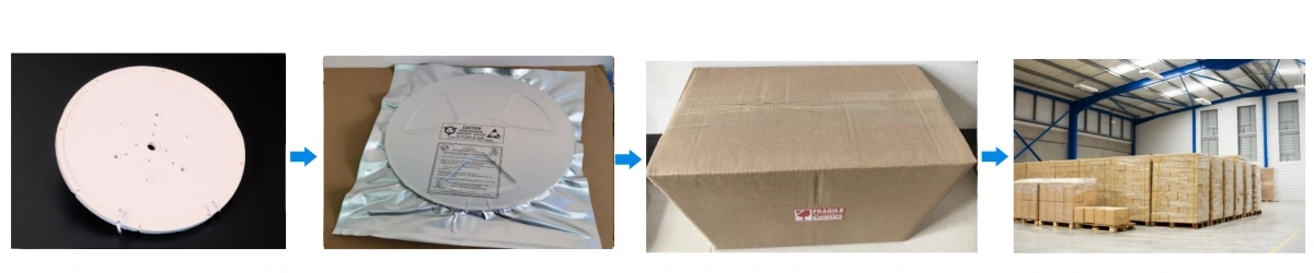
Alumina Ceramic Semiconductor Parts Packaging
- Components are individually separated using soft protective films or foam layers to reduce surface contact and chipping risk.