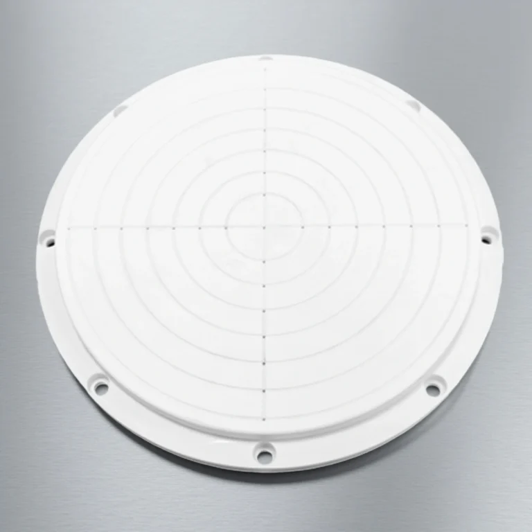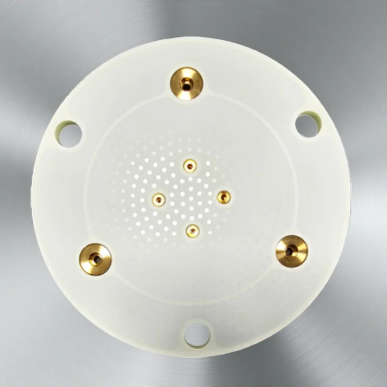
Aluminum nitride ceramic electrostatic chucks are dielectric wafer chucks that combine a high thermal conductivity AlN body with built-in electrodes and gas distribution channels to clamp, heat and cool wafers during plasma and vacuum processes. Electrostatic chucks are widely used in plasma etching, chemical vapour deposition (CVD), physical vapour deposition (PVD) and ion implantation equipment because they hold the wafer securely while allowing precise temperature control and backside gas cooling
Aluminum Nitride Ceramic Electrostatic Chuck Benefits
-
High heat-flux handling with AlN body
The aluminum nitride ceramic body supports high thermal conductivity levels, which helps the chuck handle high plasma power densities while keeping wafer temperature more uniform across the surface. -
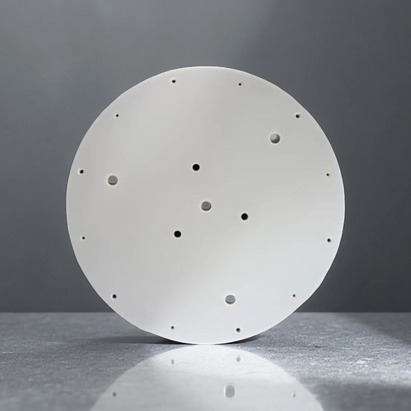
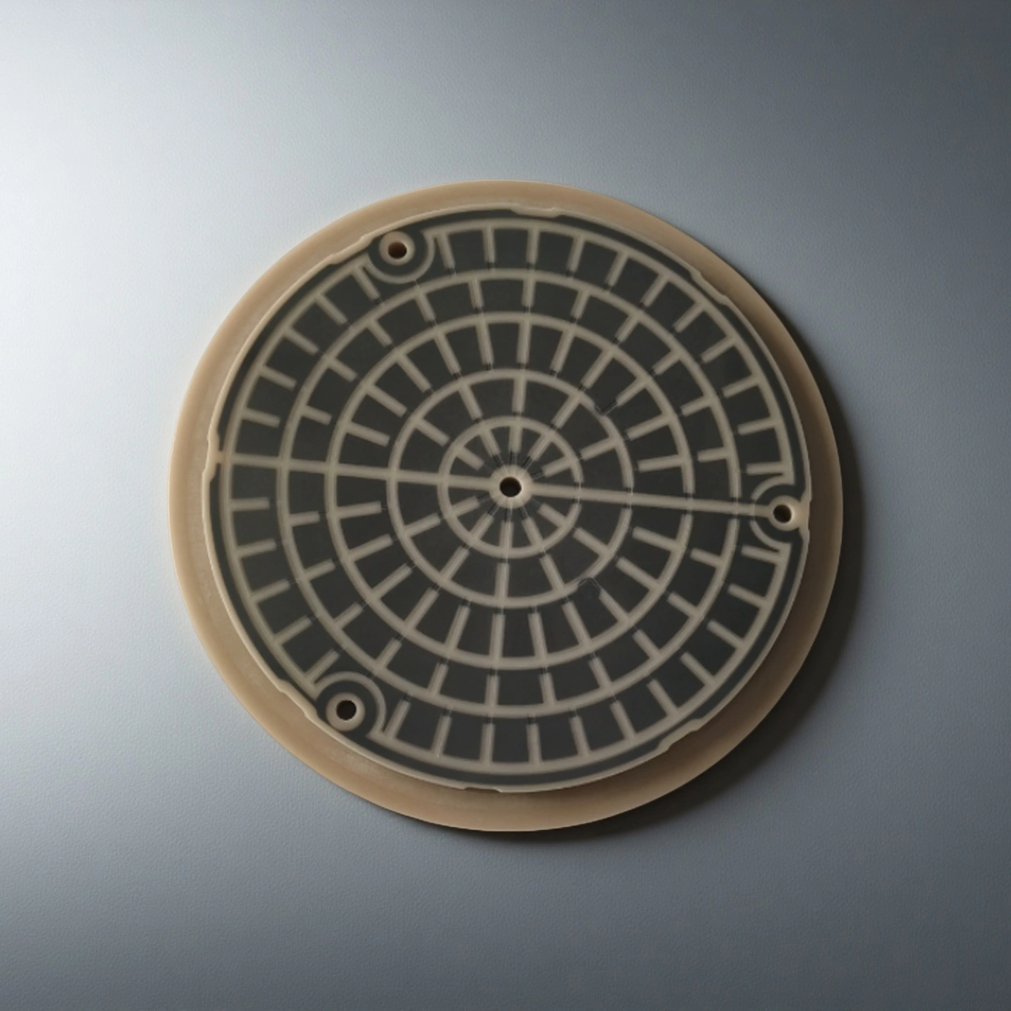
Integrated temperature control structure
The electrostatic chuck can incorporate multi-zone heater layouts, helium backside cooling grooves and embedded sensor holes to support tight wafer temperature uniformity targets used in semiconductor processing. -
Stable electrostatic clamping performance
The ceramic dielectric stack and electrode layout are designed to provide consistent chucking force, controlled release behaviour and good insulation under typical process voltages and frequencies used in plasma tools. -
Low particle and plasma compatible surface
The polished AlN surface and controlled surface features help limit particle generation and are compatible with halogen-based plasma chemistries used in etch and CVD chambers. -
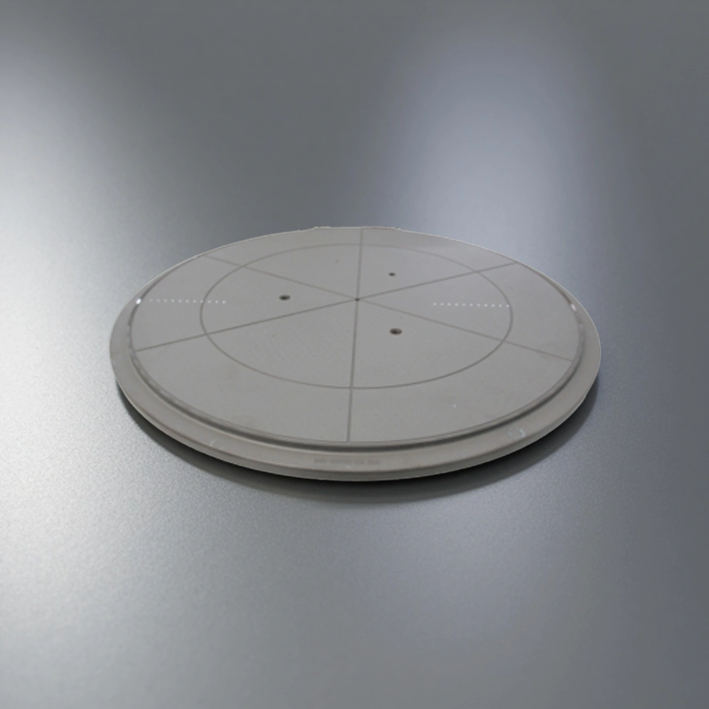
Platform-specific geometries
The aluminum nitride ceramic electrostatic chuck can be machined and ground to match specific chamber interfaces, lift-pin layouts and seal surfaces, which supports drop-in use on existing tool platforms and customized systems.
Aluminum Nitride Electrostatic Chuck Properties
| Property Content | Unit | Unit | ALN-170 | ALN-200 | ALN-230 |
| Basic Properties | Color | gray | light yellow | light yellow | |
| Density | g/cm³ | 3.2-3.3 | 3.2-3.3 | 3.2-3.3 | |
| Surface Roughness | μm | 0.2-0.75 | 0.2-0.75 | 0.2-0.8 | |
| Camber | length ‰ | ≤3‰ | ≤3‰ | ≤3‰ | |
| Hardness | HV | 1100 | 1100 | 1100 | |
| Thermal Properties | Max Operating Temperature | °C | 1100 | 1100 | 1100 |
| Thermal Conductivity | W/m·K | 170-190 | 190-220 | 220-230 | |
| Coefficient of Thermal Expansion | 10⁻⁶/K(20-400°c) | 4-5 | 4-5 | 4-5 | |
| Coefficient of Thermal Expansion | 10⁻⁶/K(400-800°c) | 5-6 | 5-6 | 5-6 | |
| Mechanical Properties | Flexural Strength | MPa | 300-400 | 350-450 | 400-500 |
| Tensile Strength | MPa | 200-300 | 250-350 | 280-380 | |
| Compressive Strength | MPa | 2000-3000 | 2200-3200 | 2500-3500 | |
| Electrical properties | Dielectric Constant | at 1MHz | 8-9 | 8-9 | 8-9 |
| Dielectric strength | KV/mm | ≥15 | ≥15 | ≥15 | |
| Volume resistivity | 20℃ Ω.cm | ≥1014 | ≥1014 | ≥1014 |
AlN Ceramic Electrostatic Chuck Specifications
| Item No. | Diameter (mm) | Thickness (mm) | Purity |
| AT-AIN-JD1001 | Customize | ||
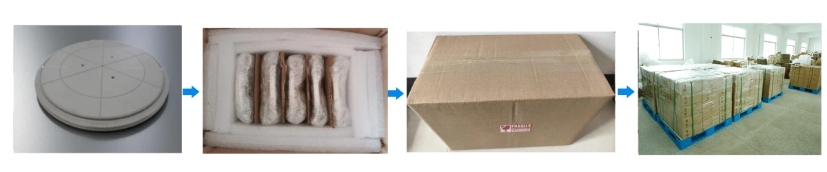
Aluminum Nitride Electrostatic Chuck Packaging
- Each aluminum nitride ceramic electrostatic chuck is first cleaned and packed in a cleanroom-compatible bag to limit particle contamination during shipping.