High Purity Alumina Polishing Plate for Wafer CMP Planarization

A High Purity Alumina Polishing Plate is a dense Al₂O₃ ceramic CMP platform or lapping plate supplied as solid or ring-type discs, typically in diameters from about 150 mm to 360 mm and thickness 20–45 mm, with flatness, slot pattern and mounting features tailored to specific wafer polishing tools.

Catalogue No. AT-HP-PT01
Material Al₂O₃
Purity  99%-99.99%
Density 3.8–3.9 g/cm³
Vickers Hardness 15–18 GPa
24H Standard Dispatch
Small Batch Support OEM
Factory Direct
Expert Engineering Support

A High Purity Alumina Polishing Plate is a dense Al₂O₃ (alumina) ceramic plate used as the rigid base surface in wafer CMP tools, lapping machines and precision polishing equipment. It is typically made from about 99.5%–99.7% alumina and machined to tight flatness so that polishing pads and slurries can planarize silicon, SiC, sapphire and other substrates with controlled thickness, low contamination and stable removal uniformity.


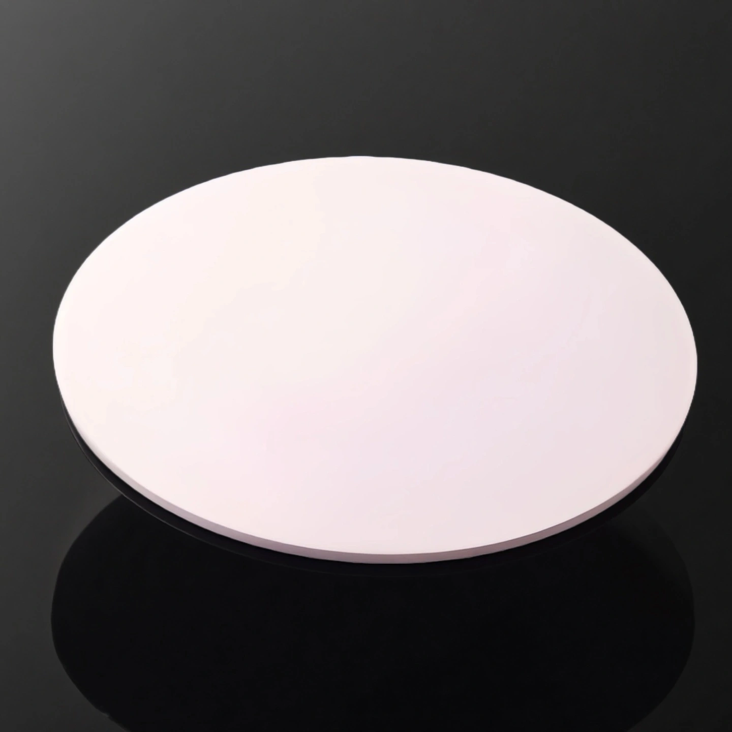
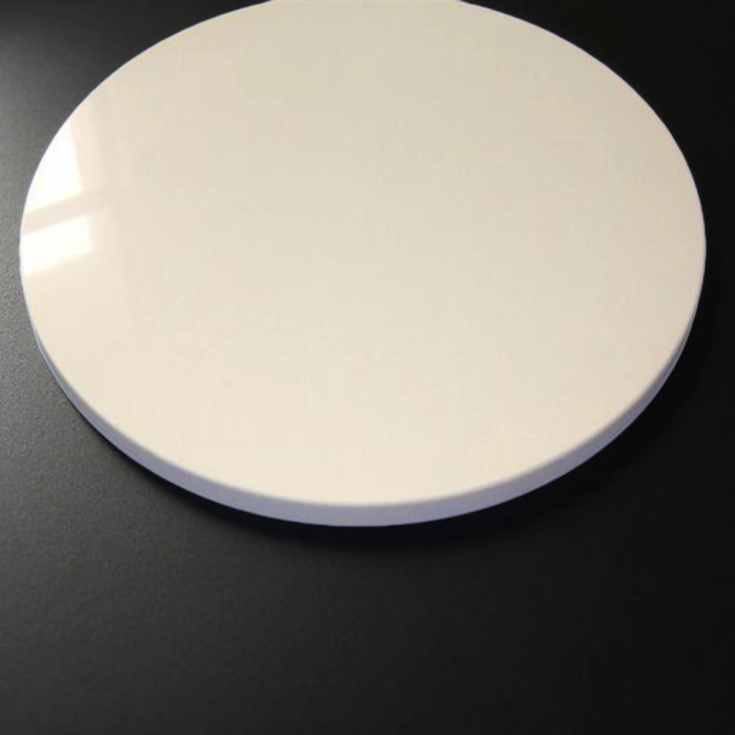
High Purity Alumina Polishing Plate Benefits

  • Dimensional stability under wafer load
    High flexural strength and elastic modulus help the high purity alumina polishing plate maintain global flatness and local planarity when carriers and pads apply pressure on 150–300 mm wafers. This reduces thickness variation and edge roll-off across the batch, even after long CMP or lapping campaigns.

  • Wear resistance in abrasive chemistries
    The high hardness and dense microstructure of alumina give the polishing plate a slow, predictable wear rate when working with silica, alumina or diamond slurries. This allows longer pad and plate life between refurbishing steps and helps keep the removal rate drift under control.

  • Low contamination of the wafer surface
    High purity Al₂O₃ and a controlled surface finish minimise metallic contamination and loose particles from the plate itself. This supports defect control on sensitive device wafers and reduces the risk of adding particles that would otherwise show up as scratches or embedded defects.

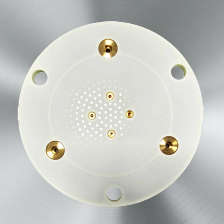
  • Customizable geometry for different tools
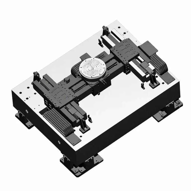
    Outer and inner diameters, ring width, groove layout, back-side pockets and mounting features can be defined according to each CMP or lapping tool. This makes it easier to retrofit existing polishers, wafer reclaim tools and pilot lines without redesigning the whole platform.

  • Compatibility with multiple substrate types
    The same high purity alumina polishing plate concept can be adapted for silicon, SiC, sapphire, glass and advanced ceramic substrates by adjusting pad type, groove pattern and slurry chemistry. One plate family can therefore support several process recipes across different product lines.


High Purity Alumina Ceramic Polishing Plate Properties

Property Unit 99.5% Al₂O₃ 99.6% Al₂O₃ 99.7% Al₂O₃ 99.8% Al₂O₃ 99.9% Al₂O₃ 99.99% Al₂O₃
Alumina content % 99.5 99.6 99.7 99.8 99.9 99.99
Density g/cm³ 3.89 3.91 3.92 3.93 3.94 3.98
Open porosity % 0
Color Ivory Ivory Ivory Ivory Ivory Ivory
Water absorption % 0 0 0 0 0
Young’s modulus (Elastic modulus) GPa 375 356 357 358 359 362
Shear modulus GPa 152
Bulk modulus GPa 228
Poisson’s ratio 0.22
Compressive strength MPa 2600 2552 2554 2556 2558 2570
Flexural strength MPa 379 312 313 314 315 320
Fracture toughness MPa·m¹ᐟ² 4
Hardness GPa 14.1 (≈1440 kg/mm²) 23 24 25 26 30
Thermal conductivity W/m·K 35 32–37 33–38 34–39 35–40 36–42
Thermal shock resistance ΔT °C 222 223 224 225 228
Maximum use temperature (no load) °C ≤1750 1755 1760 1765 1770 1800
Coefficient of thermal expansion 10⁻⁶/°C 8.4
Specific heat J/kg·K 880
Volume resistivity Ω·cm >1×10¹⁴ >1×10¹⁴ >1×10¹⁴ >1×10¹⁴ >1×10¹⁴ >1×10¹⁴
Dielectric constant (relative permittivity) 9.8 9.83 9.84 9.85 9.86 9.92
Dielectric strength kV/mm 16.9 23.2 23.4 23.6 23.8 24
Dissipation factor (loss factor @ 1 kHz) 0.0002


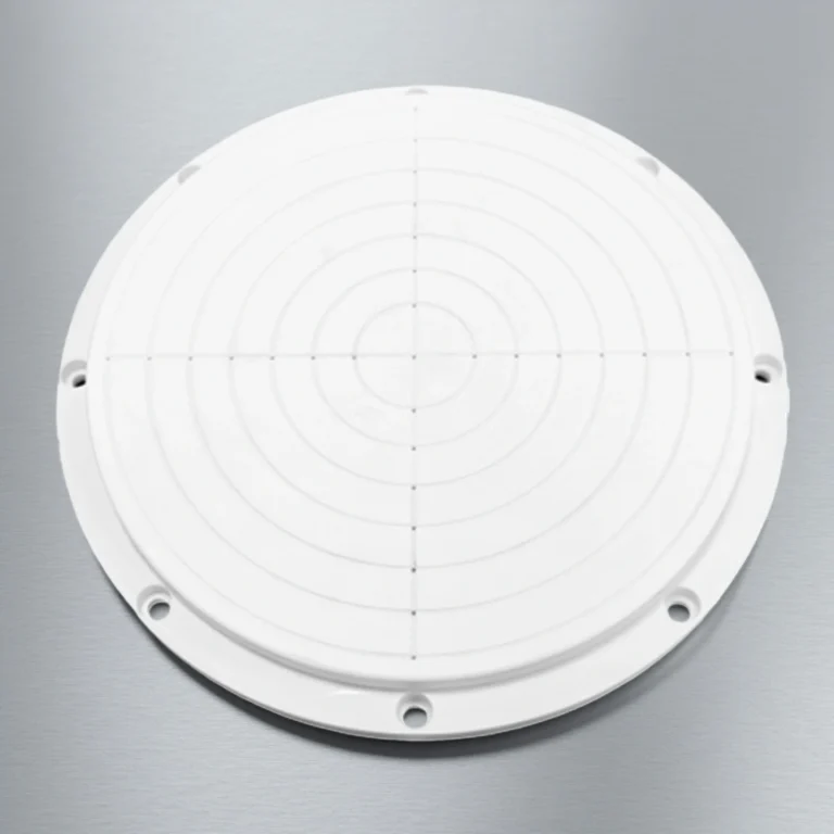
High Purity Alumina Polishing Plate Specification

High Purity Alumina Polishing Plate
Item No. Diameter (mm) Thickness (mm)
AT-HP-PT01 Customize


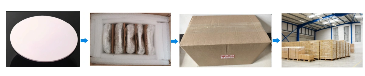
High Purity Alumina Polishing Plate Packaging

  • Each high purity alumina ceramic grinding disc is placed in a custom foam or soft-pad tray that supports the full surface and edges to minimise impact and chipping.

High Purity Alumina Ceramic Grinding Disc Packaging

Application Scenarios — High Purity Alumina Polishing Plate

  • CMP Tools for Silicon Wafer Planarization and Reclaim

    ✅Key Advantages

    1. Uniform wafer thickness control — High stiffness and flatness help the polishing plate support pad and wafer pressure so that post-CMP thickness variation stays within tight process windows.

    2. Stable performance over long runs — Wear-resistant alumina and controlled groove patterns keep slurry distribution and pad contact stable for extended tool uptime.

    3. Low risk of particle-induced defects — High purity ceramics and smooth surfaces limit plate-generated particles that could add defects to sensitive device wafers.

    ✅ Problem Solved

    A wafer manufacturer operating 200 mm and 300 mm CMP tools faces yield loss when metallic plates deform or corrode, leading to non-uniform topography and higher defect counts. Industry data show that CMP is a critical bottleneck and that unplanned downtime can cost large fabs hundreds of thousands of dollars per hour. By replacing metallic platforms with high purity alumina polishing plates specified for flatness, groove pattern and stiffness, the plant can stabilise planarization behaviour, cut unplanned plate replacement events and keep CMP modules running closer to their planned uptime, supporting both yield and capacity.

  • Sapphire and SiC Substrate Polishing for Power Devices

    ✅Key Advantages

    1. Rigid base for hard, brittle substrates — The alumina polishing plate provides a stiff support so that sapphire and SiC wafers see controlled pressure without local bending.

    2. Compatible with aggressive slurries — Chemical stability against common oxidisers and abrasives helps the plate withstand the chemistries used for wide-bandgap CMP.

    3. Geometry suited to large-area substrates — Custom diameters, ring width and groove configurations allow uniform removal on larger or thicker power device substrates.

    ✅ Problem Solved

    SiC and sapphire substrate producers often report that their CMP modules are sensitivity points for warp, bow and surface defect control. When the polishing table lacks stiffness or wears unevenly, bow and surface defects can move outside allowed ranges and scrap rates increase. Market and technical data underline that SiC CMP costs are significant in the wafer cost structure. Using a high purity alumina polishing plate with defined flatness, ring geometry and groove layout allows process engineers to hold removal uniformity and surface quality more tightly, reducing rework and supporting downstream epitaxy yield.

  • R&D and Pilot CMP Lines, Equipment Refurbishment and Service

    ✅Key Advantages

    1. Flexible geometry for experimental recipes — Custom diameters, slot patterns and surfaces make it easier to design polishing plates for new materials and process windows.

    2. Support for mixed wafer sizes — Plates can be dimensioned for 100–200 mm or 150–300 mm test wafers in pilot tools with quick change-over.

    3. Useful for refurbishment and upgrade projects — Replacement alumina polishing plates can be tailored to extend the life of legacy CMP or lapping equipment.

    ✅ Problem Solved

    Engineering centres and service companies often work with older CMP tools or customised lapping machines where the original polishing plate is no longer available. At the same time they need to evaluate new materials like SiC, GaN or advanced packaging wafers. The customer must control cost and lead time while maintaining technical capability. By specifying a high purity alumina polishing plate to fit the legacy tool—matching existing bolt patterns and pad layouts—ADCERAX enables those teams to keep their equipment productive and to adapt it to new processes without redesigning the entire platform.

Use Guide — High Purity Alumina Polishing Plate

  • Installation

    1. Inspect the polishing plate for chips or cracks before installation; do not use any plate with visible damage.
    2. Clean the machine mounting surface and remove all residual pad adhesive, corrosion or debris.
    3. Place the high purity alumina polishing plate onto the spindle or base using lifting tools if necessary; avoid striking the edges.
    4. Align keyways, pins or bolt holes with the machine layout; tighten bolts gradually in a cross pattern to minimise stress concentration.
    5. Verify run-out and flatness with a dial indicator or other metrology before installing pads or rings.

  • Operation

    1. Select pads, rings and slurry types according to the substrate and process; confirm that pad adhesives are compatible with alumina surfaces.
    2. Ramp up platen speed and pressure slowly on first use of a new plate to confirm stable mechanical behaviour.
    3. Monitor removal rate, wafer topography and temperature trends; if non-uniformity appears, check plate flatness and groove condition.
    4. Avoid excessive over-pressure or sudden recipe changes that may overload the plate or create localised wear regions.

  • Cleaning

    1. After each batch or shift, flush slurry and debris from the pad and plate surface with process water or approved cleaning fluid while rotating slowly.
    2. At pad change, remove adhesive residue from the plate using non-metallic scrapers and compatible solvents; do not use metal blades that can scratch the ceramic.
    3. Periodically inspect grooves and channels for blockage; clear any packed slurry carefully to keep uniform flow.

  • Storage

    1. When a plate is removed from the machine, clean it, dry it thoroughly and place it in a padded tray that supports both surfaces and edges.
    2. Store plates flat, with protective interlayers between stacked units; avoid direct ceramic-to-ceramic contact.
    3. Keep storage areas dry, clean and away from heavy traffic or vibration.

  • Typical Misuse Points and Solutions

    1. Issue: Edge chipping during handling.

    Cause: Lifting by hand from one side or bumping against metal fixtures.
    Solution: Use lifting aids or two-person handling for larger plates. Keep soft pads around the installation area and inspect the edges routinely.

    2. Issue: Uneven pad wear or local hot spots.

    Cause: Non-uniform slurry distribution or misaligned carriers on the alumina polishing plate.
    Solution: Check carrier planarity and pressure distribution, clean and recut grooves as needed, and verify slurry feed positions.

    3. Issue: Wafer planarization drift over time.

    Cause: Plate flatness change from cumulative wear or over-tightened mounting bolts.
    Solution: Schedule regular plate metrology, adjust bolt torque, and re-lap or replace the high purity alumina polishing plate when flatness falls outside limits.

High Purity Alumina Polishing Plate FAQ

  1. Q: What purity level is used for the High Purity Alumina Polishing Plate?
    A: The plates are based on high purity alumina grades typically around 99.5–99.7% Al₂O₃ to limit contamination and deliver stable mechanical properties.
  2. Q: How does a ceramic polishing plate differ from a metal polishing table in CMP?
    A: High purity alumina polishing plates provide higher hardness, better corrosion resistance and more stable flatness, while metal tables can deform, corrode and generate unwanted particles.
  3. Q: What wafer sizes can a High Purity Alumina Polishing Plate support?
    A: Typical designs cover 150, 200 and 300 mm wafers, with custom diameters and ring geometries available for other sizes or special carriers.
  4. Q: Can the High Purity Alumina Polishing Plate be used in both CMP and simple lapping systems?
    A: Yes, the same alumina plate concept can be adapted as a CMP table with pads and slurry or as a lapping plate with appropriate abrasives and process controls.
  5. Q: How long does a High Purity Alumina Polishing Plate typically last?
    A: Service life depends on pad type, slurry, wafer load and recipe; in general, alumina plates are selected to extend replacement intervals compared with metal or polymer-based tables under similar conditions.

Customer Reviews – High Purity Alumina Polishing Plate

  • ⭐️⭐️⭐️⭐️⭐️
    We adopted high purity alumina polishing plates on one reclaim line to replace worn metal tables. After the change, removal uniformity and wafer bow control stayed much more stable over the full pad life.
    -- Michael T., Process Engineer, Wafer Reclaim Service, USA
  • ⭐️⭐️⭐️⭐️⭐️
    ADCERAX supplied alumina polishing plates machined to our legacy bolt patterns and groove designs. The dimensions matched our drawings, so installation on refurbished CMP tools was straightforward.
    -- Sara K., Operations Manager, CMP Tool Refurbishment Company, Germany
  • ⭐️⭐️⭐️⭐️⭐️
    For several mid-size customers we needed an alternative source of ceramic wafer polishing plates. Working directly with the ADCERAX factory gave us flexibility on ring forms and allowed small pilot batches before stocking more sizes.
    -- Hiroshi Y., Technical Buyer, Semiconductor Equipment Trader, Japan
  • ⭐️⭐️⭐️⭐️⭐️
    The custom high purity alumina polishing plate we ordered has been used for SiC substrate trials for months. Flatness and groove quality are stable, so we have not had to pause experiments to rework the table.
    -- Daniel R., R&D Line Supervisor, Power Device Substrate Lab, France
customize size

Custom — High Purity Alumina Polishing Plate

ADCERAX supplies high purity alumina polishing plates as both standard designs and fully custom parts so that each plate matches the geometry, pad configuration and slurry flow pattern of the CMP or lapping tool.

1. Outer and inner diameters

  • Typical outer diameters: approx. Ø150, Ø200, Ø300, Ø360 mm; larger sizes possible after engineering review.
  • Inner diameters and ring widths matched to pad design and carrier size.

2. Thickness and tolerances

  • Common thickness range: 20–45 mm.
  • Thickness tolerance down to ±0.05–0.10 mm, tighter by agreement.

3. Flatness and run-out targets

  • Global flatness specified according to wafer size and process (from tens of micrometres downward).
  • Parallelism and run-out are defined for the mounting interface.

4. Surface texture and pattern

  • Pad-contact surface prepared as solid, cross-hatched, spiral or radial grooved pattern.
  • Surface roughness tailored to pad bonding and slurry distribution requirements.

5. Edge and corner design

  • Chamfers or radii on outer and inner edges to reduce chipping during handling and operation.

6. Mounting details

  • Bolt hole patterns, keyways, alignment pins, recesses or back-side pockets to suit each CMP polisher or lapping machine.

Related Products

ADCERAX - Your Trusted Advanced Ceramics Manufacturing Partner

Direct factory manufacturing with comprehensive ceramic materials expertise and global supply capabilities

Direct Factory Manufacturing

China-based ceramic materials production facility with state-of-the-art equipment

Engineering Team

Experienced professionals in advanced ceramics applications and custom design

Quality Control

Strict quality control standards for technical ceramics manufacturing and quality management

Global Supply Chain

Serving customers worldwide with technical ceramics and rapid response

24/7 Technical Support

Round-the-clock support for ceramic components inquiries and technical assistance

500+ Satisfied Customers

Trusted by global customers for advanced ceramic materials and precision components

Get in touch with us

Our team will be happy to respond to you in less than 24 hours.

Adcerax's factory

Quick Quotation

*Our team will answer your inquiries within 24 hours.

*Your information will be kept strictly confidential.

Ready to Solve Your Engineering Challenge?

Partner with ADCERAX for reliable, high-performance advanced ceramic solutions. Our engineers are ready to discuss your project.

E-mail

info@adcerax.com

Phone

+(86) 0731-74427743 | WhatsApp: +(86) 19311583352

Response Time

Within 24 hours

Quick Quote

The more details you provide, the faster we can quote.

*We respond within 24 hours. All inquiries are confidential.

Download Catalog

Get Your Custom Sulution

The more details you provide, the faster we can respond.

customize size

*We respond within 24 hours. All inquiries are confidential.

Download Catalog