Alumina Substrate Properties define whether electronic systems endure thermal stress or fail prematurely. Consequently, overlooking material behavior often results in instability, degraded performance, and unexpected reliability losses.
Alumina Substrate Properties govern electrical insulation, thermal transport, and mechanical stability across power electronics, LED packaging, and thick-film circuit systems. Therefore, understanding how these properties interact at system level is essential for engineers designing reliable electronic assemblies under thermal, electrical, and mechanical constraints.

Before examining individual material parameters in detail, it is necessary to establish how Alumina Substrate Properties function within electronic systems as an integrated whole. Otherwise, isolated property values risk being misinterpreted outside their true engineering context.
Alumina Substrate as a Functional Electronic Component
From an engineering perspective, an alumina substrate is not a passive material layer but an active functional component within electronic assemblies. Moreover, it simultaneously performs electrical insulation, thermal redistribution, and mechanical load transfer under continuous operational stress.
-
Electrical isolation under elevated voltage gradients
Alumina substrates routinely sustain dielectric strengths exceeding 10–15 kV/mm, which enables compact conductor spacing in power modules and control circuits. Consequently, electrical insulation becomes a structural design parameter rather than a secondary safety feature. -
Thermal redistribution across localized heat sources
With a typical thermal conductivity around 20–30 W/m·K, alumina substrates moderate temperature gradients between hotspots and surrounding structures. As a result, they reduce localized thermal shock even when absolute heat dissipation remains limited. -
Mechanical support under constrained assembly conditions
Alumina substrates exhibit flexural strengths commonly ranging from 300–400 MPa, allowing them to act as rigid load-bearing elements during soldering, wire bonding, and encapsulation. Therefore, mechanical integrity directly influences long-term electrical and thermal stability.
In practical engineering environments, these three functions are inseparable. Accordingly, treating Alumina Substrate Properties as independent material descriptors rather than integrated system enablers often leads to design margins that appear adequate on paper but fail under real operating conditions.
Fundamental Material Properties of Alumina Substrates
Alumina Substrate Properties form the quantitative foundation for all subsequent system-level behavior. Moreover, these intrinsic parameters establish the physical boundaries within which thermal, electrical, and mechanical design decisions must operate.
At material level, alumina substrates are defined not by a single dominant parameter but by a coordinated set of properties. Consequently, engineers evaluating alumina must understand how each property contributes independently while also anticipating their combined influence under operating stress.
Thermal Transport Characteristics of Alumina
Thermal transport behavior determines how efficiently heat migrates away from localized sources. Therefore, alumina’s role in thermal regulation must be evaluated using multiple interrelated thermal parameters rather than thermal conductivity alone.
In practice, dense alumina substrates typically exhibit a thermal conductivity between 20 and 30 W/m·K at room temperature, decreasing gradually as temperature rises. Meanwhile, heat capacity values near 750–900 J/kg·K moderate transient temperature spikes during power cycling. Together, these characteristics yield a thermal diffusivity on the order of 8–12 mm²/s, which governs response speed rather than steady-state heat flow.
During design validation, engineers often observe that alumina substrates delay peak temperature propagation by several seconds compared to high-conductivity ceramics. As a result, thermal gradients become less abrupt, reducing instantaneous thermo-mechanical stress within bonded interfaces. This controlled heat spreading behavior often improves long-term reliability, even when maximum heat dissipation appears lower on datasheets.
| Thermal Property | Typical Value Range | Measurement Context |
|---|---|---|
| Thermal conductivity (W/m·K) | 20–30 | 25 °C, dense alumina |
| Specific heat capacity (J/kg·K) | 750–900 | 25–500 °C |
| Thermal diffusivity (mm²/s) | 8–12 | Derived property |
| Maximum service temperature (°C) | 1500–1600 | Oxidizing atmosphere |
Electrical Insulation Characteristics
Electrical insulation performance defines the safety envelope for alumina substrates operating under high voltage or high frequency conditions. Consequently, dielectric behavior must be assessed across both field strength and environmental variation.
Dense alumina substrates routinely demonstrate dielectric strengths exceeding 10–15 kV/mm, enabling compact conductor spacing without premature breakdown. In parallel, relative permittivity values typically range from 9.0 to 9.8, while dielectric loss factors remain below 0.001 at 1 MHz for high-purity grades. These values ensure stable electric field distribution and limited energy dissipation under alternating fields.
In laboratory testing, engineers frequently note that dielectric strength remains stable up to 300–400 °C before gradual degradation occurs. Accordingly, alumina substrates provide a predictable insulation margin across wide temperature ranges. This stability is especially critical in power electronics and sensing circuits, where insulation failure often triggers cascading system damage rather than localized faults.
| Electrical Property | Typical Value Range | Test Condition |
|---|---|---|
| Dielectric strength (kV/mm) | 10–15 | Room temperature |
| Relative permittivity (–) | 9.0–9.8 | 1 MHz |
| Dielectric loss (tan δ) | ≤0.001 | 1 MHz |
| Volume resistivity (Ω·cm) | >10¹⁴ | 25 °C |
Mechanical Resistance Characteristics
Mechanical resistance defines how alumina substrates tolerate external loads and internally generated stresses. Therefore, mechanical properties directly influence survivability during assembly and service.
Typical alumina substrates exhibit flexural strengths between 300 and 400 MPa, accompanied by an elastic modulus of approximately 300–380 GPa. Fracture toughness values generally remain within 3–4 MPa·m¹ᐟ², reflecting the inherently brittle nature of ceramic materials. Although plastic deformation is absent, elastic strain capacity allows alumina to withstand controlled mechanical loading.
In manufacturing environments, engineers often encounter microcrack initiation during cutting or drilling operations when stress concentrations exceed local strength limits. Consequently, mechanical properties must be interpreted alongside processing methods, as identical nominal strength values can yield vastly different outcomes depending on geometry and constraint. Recognizing these limits early prevents downstream failure during solder reflow or encapsulation.
| Mechanical Property | Typical Value Range | Relevance |
|---|---|---|
| Flexural strength (MPa) | 300–400 | Load-bearing capacity |
| Elastic modulus (GPa) | 300–380 | Stiffness under constraint |
| Fracture toughness (MPa·m¹ᐟ²) | 3–4 | Crack resistance |
| Hardness (HV) | 1500–1800 | Machining sensitivity |
Summary of Fundamental Alumina Substrate Properties
| Property Domain | Governing Parameters | System-Level Implication |
|---|---|---|
| Thermal | Conductivity, heat capacity, diffusivity | Temperature gradient control |
| Electrical | Dielectric strength, permittivity | Insulation reliability |
| Mechanical | Strength, modulus, toughness | Structural integrity |

Coupled Property Interactions in Alumina Substrates
Alumina Substrate Properties rarely act in isolation under real operating conditions. Moreover, system-level reliability is governed by how thermal, electrical, and mechanical properties interact simultaneously under constraint, cycling, and environmental exposure.
At this stage, understanding coupled behavior becomes essential. Otherwise, designs based solely on isolated datasheet values often underestimate stress accumulation mechanisms that only emerge when multiple properties interact over time.
Thermal Mechanical Interaction Under Cyclic Loading
Thermal mechanical coupling1 is the dominant interaction governing long-term durability in alumina substrates. Therefore, temperature variation must always be evaluated together with elastic response and thermal expansion behavior.
In dense alumina, the coefficient of thermal expansion typically lies between 6.5 and 8.0 ×10⁻⁶ K⁻¹, while the elastic modulus remains above 300 GPa. During power cycling, repeated temperature swings of 80–150 °C induce cyclic strain that cannot be plastically relaxed. Consequently, elastic strain energy accumulates at interfaces, edges, and microstructural discontinuities.
In practical power module testing, engineers frequently observe microcrack initiation after 10⁴–10⁵ thermal cycles, even when peak temperatures remain well below material limits. This phenomenon illustrates that thermal conductivity alone cannot predict durability, as fracture behavior is controlled by the combined action of expansion mismatch, stiffness, and geometric constraint.
| Coupled Parameters | Typical Range | Observed Effect |
|---|---|---|
| Thermal expansion (×10⁻⁶ K⁻¹) | 6.5–8.0 | Strain generation |
| Elastic modulus (GPa) | 300–380 | Stress amplification |
| Thermal cycle amplitude (°C) | 80–150 | Fatigue initiation |
| Cycle count to microcracking | 10⁴–10⁵ | Reliability threshold |
Electrical Thermal Interaction in High Power Density Conditions
Electrical and thermal properties interact strongly when alumina substrates operate under high power density. Consequently, insulation performance cannot be assessed independently from temperature rise.
As temperature increases, alumina exhibits a gradual reduction in dielectric strength, typically decreasing by 10–20% between 25 °C and 300 °C. Simultaneously, dielectric loss increases modestly, leading to localized heating under alternating electric fields. This feedback loop is usually weak at low field strength but becomes significant above 2–3 kV/mm.
In field testing of compact power assemblies, engineers often report insulation degradation occurring preferentially near thermal hotspots rather than uniformly across the substrate. This observation confirms that thermal gradients accelerate electrical aging, even when average operating conditions appear conservative.
| Electrical Thermal Coupling | Quantitative Trend | Design Implication |
|---|---|---|
| Dielectric strength change | −10–20% to 300 °C | Reduced safety margin |
| Dielectric loss increase | <2× baseline | Local heat generation |
| Electric field intensity (kV/mm) | 2–3 | Aging acceleration |
| Hotspot temperature rise (°C) | 30–60 | Failure localization |
Mechanical Process Interaction During Fabrication
Mechanical properties interact with processing steps long before a substrate enters service. Therefore, fabrication-induced damage must be considered part of the coupled property framework.
During cutting, drilling, or slotting, localized stresses can exceed 400 MPa, temporarily surpassing the flexural strength of alumina. Although macroscopic fracture may not occur, microcracks with lengths below 50 μm are commonly introduced at edges and hole walls. These defects remain dormant until activated by thermal or electrical stress.
In post-assembly failure analysis, engineers frequently trace crack propagation back to machining features rather than bulk material flaws. This pattern demonstrates that processing history directly conditions coupled property response, linking manufacturing choices to long-term reliability.
| Processing Interaction | Typical Scale | Long-Term Impact |
|---|---|---|
| Machining stress (MPa) | >400 | Microcrack initiation |
| Microcrack size (μm) | <50 | Latent defect |
| Edge stress concentration | High | Crack propagation |
| Combined thermal activation | 80–150 °C cycles | Premature failure |
Summary of Coupled Property Interactions
| Interaction Type | Dominant Properties | Resulting Risk |
|---|---|---|
| Thermal mechanical | CTE, modulus, strength | Fatigue cracking |
| Electrical thermal | Dielectric strength, loss | Insulation aging |
| Mechanical process | Strength, toughness | Defect activation |

Alumina Substrate Properties in Power Electronics and Power Modules
Alumina Substrate Properties directly shape thermal stability, insulation margins, and structural endurance in power electronics. Consequently, power module reliability depends on how these properties behave under continuous electrical load and cyclic thermal stress.
In high-power assemblies, alumina substrates operate as both electrical barriers and thermal intermediaries. Therefore, their material behavior must be evaluated at module level rather than as isolated ceramic plates.
Thermal Load Management in Power Modules
Thermal load management defines whether a power module maintains junction stability or accumulates irreversible damage. Accordingly, alumina substrates must control temperature gradients rather than simply dissipate heat.
In power modules, alumina substrates typically operate with heat flux levels ranging from 10 to 50 W/cm², depending on device density and cooling strategy. With thermal conductivity near 25 W/m·K, alumina spreads heat laterally while limiting steep temperature spikes at die edges. As a result, peak junction temperature rise is often reduced by 8–15 °C compared with thinner insulating alternatives.
During accelerated life testing, engineers frequently observe that alumina substrates delay hotspot migration across copper traces and solder joints. This moderated thermal response stabilizes interfacial stresses, particularly during rapid load changes. Consequently, alumina substrates contribute to predictable thermal behavior even when absolute thermal conductivity appears moderate.
| Thermal Parameter | Typical Range | Module-Level Effect |
|---|---|---|
| Heat flux (W/cm²) | 10–50 | Thermal stress driver |
| Thermal conductivity (W/m·K) | 20–30 | Lateral heat spreading |
| Junction temperature reduction (°C) | 8–15 | Stress mitigation |
| Operating temperature window (°C) | −40 to 200 | Stability range |
Electrical Isolation Under High Voltage Stress
Electrical isolation is a defining requirement for power electronics. Therefore, alumina substrates must preserve dielectric integrity under combined electric field and thermal exposure.
In typical power modules, electric field intensities across alumina substrates range from 1 to 3 kV/mm. With dielectric strength exceeding 10 kV/mm, alumina maintains a safety factor above 3× under nominal conditions. However, elevated temperatures gradually reduce this margin, particularly above 250 °C.
In field evaluations, engineers often detect partial discharge activity originating near metallization edges rather than uniform breakdown. This behavior reflects the interaction between electric field concentration and thermal gradients, not intrinsic material weakness. Accordingly, alumina substrates enable robust insulation when geometry and metallization design respect local field amplification effects.
| Electrical Parameter | Typical Range | Reliability Impact |
|---|---|---|
| Electric field (kV/mm) | 1–3 | Operating stress |
| Dielectric strength (kV/mm) | 10–15 | Safety margin |
| Temperature threshold (°C) | 250–300 | Margin reduction |
| Partial discharge onset | Edge-localized | Design-sensitive |
Structural Endurance During Power Cycling
Structural endurance governs long-term survival in power modules exposed to repetitive load variation. Consequently, alumina substrates must resist fatigue driven by thermal expansion mismatch.
Alumina substrates experience cyclic strain when power cycling induces temperature swings of 80–150 °C. With elastic modulus above 300 GPa and limited fracture toughness, these cycles generate tensile stresses at interfaces and corners. Fatigue testing commonly reveals microcrack initiation after 10⁴–10⁵ cycles, particularly near solder joints and copper edges.
In failure analysis, engineers often find that crack growth proceeds slowly until a critical length is reached. This delayed failure mode masks early damage, making alumina substrate endurance dependent on cumulative rather than instantaneous stress. As a result, conservative cycle design significantly extends module lifetime.
| Mechanical Parameter | Typical Value | Fatigue Implication |
|---|---|---|
| Temperature swing (°C) | 80–150 | Cyclic strain driver |
| Elastic modulus (GPa) | 300–380 | Stress intensity |
| Cycles to microcracking | 10⁴–10⁵ | Lifetime indicator |
| Crack propagation mode | Subcritical | Delayed failure |
Summary of Alumina Substrate Performance in Power Modules
| Performance Aspect | Governing Properties | System Outcome |
|---|---|---|
| Thermal control | Conductivity, heat capacity | Junction stability |
| Electrical isolation | Dielectric strength, permittivity | Voltage safety |
| Structural endurance | Modulus, CTE, toughness | Fatigue resistance |

Alumina Substrate Properties in LED Packaging and DPC Circuit Boards
Alumina Substrate Properties strongly influence thermal uniformity, metallization reliability, and optical stability in LED packaging. Moreover, these properties determine whether DPC2 ceramic circuit boards sustain long-term luminous performance under continuous thermal loading.
In LED systems, alumina substrates operate closer to steady-state thermal conditions than power modules. Therefore, material behavior must be assessed for heat spreading uniformity and surface compatibility rather than transient endurance alone.
Heat Dissipation Pathways in LED Assemblies
Heat dissipation in LED assemblies depends on how efficiently the substrate redistributes localized junction heat. Consequently, alumina substrates must minimize lateral temperature gradients rather than maximize bulk heat removal.
In practical LED modules, heat flux levels typically range from 2 to 10 W/cm², significantly lower than in power electronics but applied continuously over long durations. With thermal conductivity near 20–25 W/m·K, alumina substrates spread heat across the ceramic plane, reducing localized junction temperature variation by approximately 5–12 °C across densely populated LED arrays.
During thermal imaging validation, engineers often observe smoother temperature contours on alumina-based DPC boards compared with polymer substrates. This uniform heat distribution stabilizes phosphor efficiency and slows lumen depreciation, particularly in high-flux lighting applications. As a result, alumina substrates contribute directly to optical consistency rather than merely structural support.
| Thermal Parameter | Typical Range | LED System Effect |
|---|---|---|
| Heat flux (W/cm²) | 2–10 | Continuous thermal load |
| Thermal conductivity (W/m·K) | 20–25 | Lateral heat spreading |
| Junction temperature variation (°C) | 5–12 | Optical stability |
| Operating temperature (°C) | 80–180 | Long-term exposure |
Surface Condition Requirements for DPC Metallization
Surface condition governs metallization adhesion and circuit integrity in DPC ceramic boards. Therefore, alumina substrate properties must support both chemical bonding and mechanical anchoring of copper layers.
High-density alumina substrates typically present surface roughness values between Ra 0.3 and 0.8 μm after controlled polishing or lapping. This microtopography enhances copper adhesion while maintaining dimensional precision. Meanwhile, substrate density above 3.8 g/cm³ limits subsurface porosity that could otherwise weaken metallization interfaces.
In process qualification, engineers frequently correlate metallization peel strength above 8–12 N/mm with stable surface roughness and uniform grain structure. When surface conditions deviate beyond this window, delamination often initiates at thermal cycling edges, rather than within bulk copper layers. Consequently, surface property control is central to DPC reliability.
| Surface Property | Typical Value | Metallization Outcome |
|---|---|---|
| Surface roughness Ra (μm) | 0.3–0.8 | Adhesion balance |
| Substrate density (g/cm³) | >3.8 | Interface stability |
| Copper peel strength (N/mm) | 8–12 | Circuit durability |
| Metallization thickness (μm) | 100–300 | Thermal conduction |
Environmental Stability in High Flux Operation
Environmental stability defines LED lifetime under prolonged thermal and humidity exposure. Accordingly, alumina substrate properties must remain stable across combined thermal and atmospheric stress.
Dense alumina substrates exhibit water absorption below 0.1%, limiting moisture-driven dielectric variation and corrosion pathways. Under accelerated aging at 85 °C and 85% relative humidity, alumina-based DPC boards typically retain over 95% of initial insulation resistance after 1,000 hours.
In field deployments, engineers often attribute reduced lumen maintenance in LED fixtures to substrate-induced thermal gradients rather than optical material degradation. This observation highlights alumina’s role in indirectly preserving optical materials by stabilizing the thermal environment. Therefore, environmental robustness extends beyond electrical performance into optical system reliability.
| Environmental Parameter | Typical Condition | Performance Retention |
|---|---|---|
| Water absorption (%) | <0.1 | Moisture resistance |
| Damp heat exposure | 85 °C / 85% RH | Accelerated aging |
| Insulation retention (%) | >95 | Electrical stability |
| Test duration (hours) | 1,000 | Long-term indicator |
Summary of Alumina Substrate Performance in LED and DPC Systems
| Performance Aspect | Governing Properties | System Impact |
|---|---|---|
| Thermal uniformity | Conductivity, diffusivity | Lumen consistency |
| Metallization reliability | Surface roughness, density | Circuit durability |
| Environmental stability | Absorption, insulation | Lifetime extension |

Alumina Substrate Properties for Thick Film Thin Film and Sensor Circuits
Alumina Substrate Properties govern signal stability, dimensional precision, and process compatibility in thick film, thin film, and sensor circuits. Moreover, these applications amplify subtle material behaviors because electrical accuracy often depends on micrometer-scale stability rather than bulk strength.
In contrast to power and LED systems, these circuits operate at lower thermal loads. Nevertheless, long-term accuracy depends on how alumina behaves during deposition, firing, and environmental exposure.
Compatibility with Thick Film Deposition and Firing
Thick film circuits rely on predictable interaction between ceramic substrates and functional pastes. Therefore, alumina substrate properties must remain stable throughout repeated firing cycles.
In standard thick film processes, firing temperatures typically range from 850 to 950 °C, while peak dwell times extend from 5 to 15 minutes per cycle. Dense alumina substrates maintain dimensional change below 0.1% per firing, preventing cumulative misalignment across multilayer circuits. Additionally, surface roughness within Ra 0.5–1.0 μm promotes uniform paste wetting without excessive spreading.
During process trials, engineers often observe that substrates with inconsistent surface energy cause line width variation exceeding ±8% after firing. Such deviations directly affect resistor values and conductor continuity, particularly in high-density layouts. Consequently, alumina’s firing stability underpins electrical repeatability rather than merely mechanical survival.
| Thick Film Parameter | Typical Range | Process Outcome |
|---|---|---|
| Firing temperature (°C) | 850–950 | Paste sintering |
| Dimensional change (%) | <0.1 | Alignment control |
| Surface roughness Ra (μm) | 0.5–1.0 | Paste uniformity |
| Line width variation (%) | <±5 | Electrical consistency |
Electrical Stability in Sensing and Control Applications
Sensor and control circuits demand electrical stability over time rather than peak performance. Accordingly, alumina substrate properties must suppress drift under thermal and environmental fluctuations.
High-purity alumina substrates exhibit volume resistivity above 10¹⁴ Ω·cm at 25 °C, decreasing gradually with temperature yet remaining above 10¹¹ Ω·cm at 200 °C. Relative permittivity remains stable within ±2% across this range, minimizing baseline drift in capacitive and resistive sensing elements.
In field calibration scenarios, engineers frequently report that signal drift below 0.3% per 1,000 hours correlates strongly with stable dielectric behavior rather than circuit design alone. This reinforces that alumina substrates act as silent stabilizers, preserving measurement integrity across long service intervals.
| Electrical Stability Metric | Typical Value | Measurement Impact |
|---|---|---|
| Volume resistivity (Ω·cm) | >10¹⁴ (25 °C) | Leakage suppression |
| Resistivity at 200 °C (Ω·cm) | >10¹¹ | High-temp stability |
| Permittivity variation (%) | ±2 | Signal consistency |
| Long-term drift (%/1000 h) | <0.3 | Calibration retention |
Precision Machining Constraints for Circuit Integration
Precision machining defines whether alumina substrates integrate seamlessly into compact sensor and control assemblies. Therefore, mechanical properties must be evaluated in the context of micro-scale features.
Alumina substrates support laser-drilled or mechanically drilled holes as small as 100–200 μm, provided edge chipping remains below 20 μm. With hardness values between 1500 and 1800 HV, alumina resists deformation but amplifies stress concentration if tooling parameters are poorly controlled.
In prototype fabrication, engineers often detect premature cracking when slot widths fall below 300 μm without adequate edge radius. Such failures originate from combined hardness and low fracture toughness, not from bulk material defects. As a result, machining limits must be aligned with substrate properties early in layout design.
| Machining Parameter | Typical Limit | Integration Effect |
|---|---|---|
| Minimum hole diameter (μm) | 100–200 | Packaging density |
| Edge chipping (μm) | <20 | Reliability margin |
| Hardness (HV) | 1500–1800 | Tool wear sensitivity |
| Minimum slot width (μm) | ≥300 | Crack prevention |
Summary of Alumina Substrate Performance in Film and Sensor Circuits
| Performance Aspect | Governing Properties | Circuit Outcome |
|---|---|---|
| Process compatibility | Surface roughness, stability | Yield consistency |
| Electrical stability | Resistivity, permittivity | Signal accuracy |
| Integration precision | Hardness, toughness | Assembly reliability |

Before system behavior can be evaluated reliably, Alumina Substrate Properties must be traced back to manufacturing origins. Moreover, forming and sintering routes decisively condition thermal, electrical, and mechanical responses observed in service.
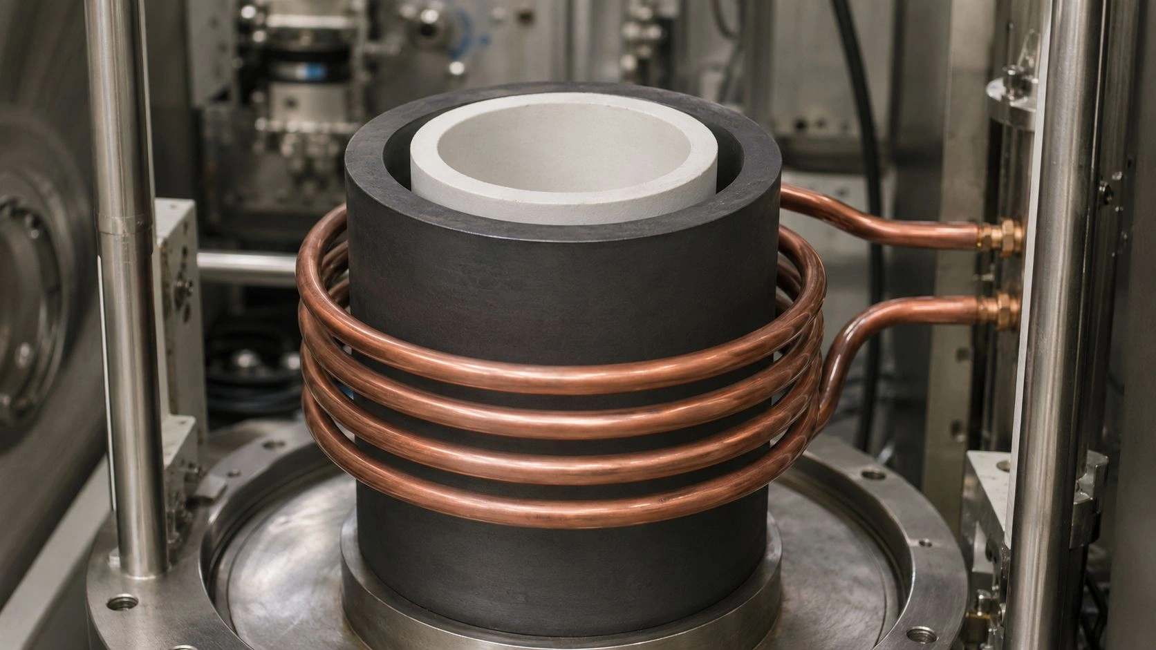
Manufacturing Processes Influencing Alumina Substrate Properties
Manufacturing processes determine how intrinsic alumina chemistry is translated into usable substrate performance. Consequently, powder preparation, forming, sintering, and post-processing steps directly shape the final property envelope delivered to electronic systems.
-
Powder preparation and particle size distribution
Alumina powder particle size typically ranges from 0.3 to 3.0 μm, and its distribution strongly influences packing density during forming. Finer powders increase green density and promote uniform sintering, while broader distributions improve packing efficiency but may induce local porosity. Excessively coarse particles often reduce final density below 3.7 g/cm³, which negatively affects dielectric strength and thermal conductivity. -
Forming routes and green body density
Common forming routes such as dry pressing, tape casting, and extrusion generate different green density profiles across the substrate. Tape-cast alumina sheets often achieve thickness uniformity within ±3–5%, whereas pressed substrates may show localized density gradients near edges. These density variations later translate into differential shrinkage, influencing flatness and residual stress after firing. -
Sintering temperature profiles and grain growth behavior
Sintering of alumina substrates typically occurs between 1500 and 1650 °C, where grain growth accelerates rapidly beyond critical dwell times. Controlled sintering maintains average grain sizes near 3–8 μm, balancing strength and fracture resistance. Over-sintering enlarges grains and reduces flexural strength, despite achieving high bulk density. -
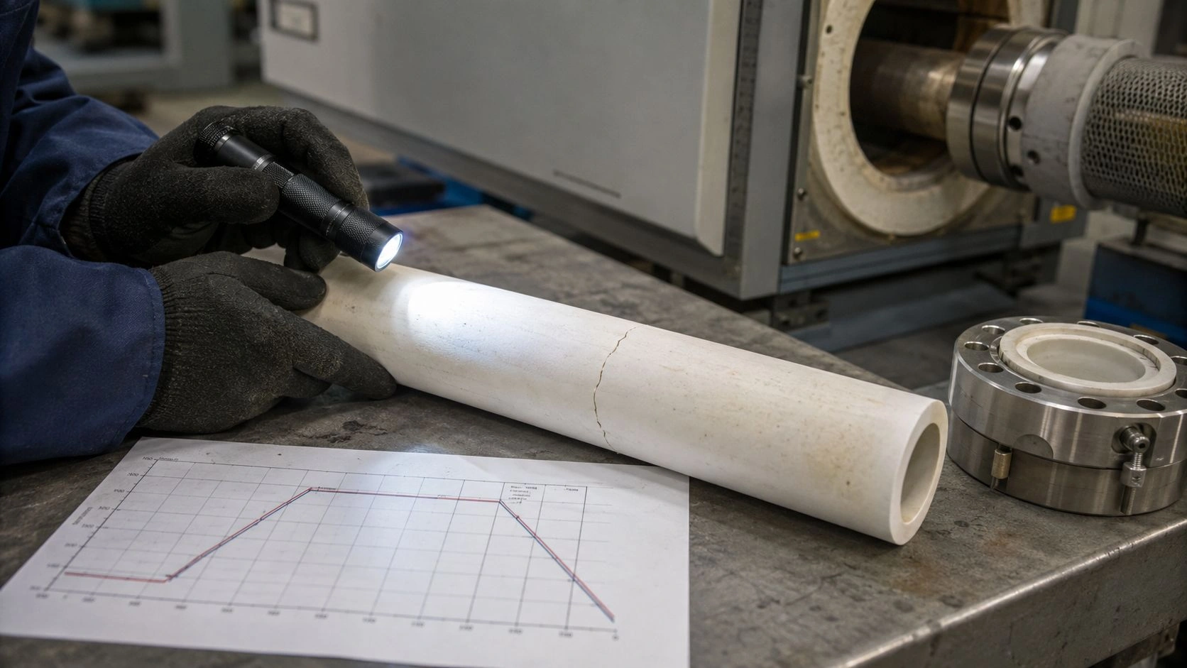
Post-sintering machining and surface conditioning
Grinding, lapping, and polishing refine final dimensions and surface roughness to Ra values between 0.3 and 1.0 μm. However, excessive material removal can introduce subsurface damage extending 10–30 μm below the surface. These latent defects often become activation sites during thermal or electrical loading, linking surface processing directly to reliability outcomes.
Taken together, manufacturing stages define a continuous property evolution rather than isolated steps. Accordingly, alumina substrate performance in electronic systems must always be interpreted through the lens of its complete manufacturing history.
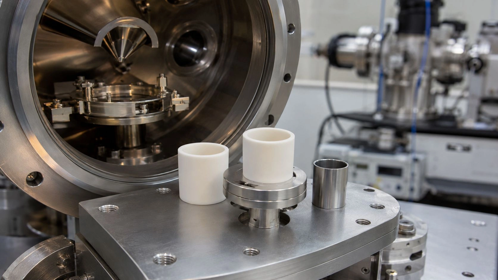
Before application-specific behavior can be fully assessed, Alumina Substrate Properties must be examined through the lens of geometry. Moreover, thickness, planar dimensions, and dimensional stability frequently impose constraints that cut across power electronics, LED packaging, and film-based circuit designs.
Structural Geometry Thickness and Dimensional Stability Considerations
Structural geometry determines how alumina substrates distribute stress, conduct heat, and maintain alignment during assembly and operation. Therefore, thickness selection and dimensional control are not secondary layout choices but primary engineering decisions.
-
Thickness dependent thermal and mechanical response
Alumina substrates are commonly produced in thickness ranges from 0.25 to 1.0 mm, with thicker sections increasing bending stiffness while simultaneously elevating thermal resistance. Consequently, substrates above 0.63 mm often reduce warpage during assembly but raise steady-state junction temperatures by 5–10 °C in compact layouts. -
Large area substrates versus small form factors
As substrate area increases beyond 50 × 50 mm, differential shrinkage and thermal gradients become more pronounced. Engineers frequently observe flatness deviations exceeding 80–120 μm on large panels after metallization or firing. These deviations complicate multilayer alignment and solder joint uniformity, particularly in DPC and thick film circuits. -
Flatness and warpage constraints in assembly processes
Typical assembly specifications require substrate warpage below 0.2% of diagonal length to ensure reliable soldering and wire bonding. Alumina’s high elastic modulus limits elastic relaxation once warpage is introduced. Therefore, geometry-induced distortion often persists through reflow and encapsulation stages unless proactively controlled.
Taken together, geometric considerations translate material properties into real-world tolerances that govern manufacturability. Accordingly, successful alumina substrate integration requires geometry to be evaluated concurrently with thermal, electrical, and mechanical performance rather than treated as a downstream adjustment.
Before final material boundaries are established, Alumina Substrate Properties must be evaluated against alternative substrate materials. Moreover, comparative assessment clarifies where alumina remains appropriate and where physical limits justify material substitution.
Comparative Properties of Alumina AlN Si3N4 and FR4 Substrates
Material comparison reveals how fundamental physical differences translate into system-level constraints. Therefore, alumina, aluminum nitride, silicon nitride, and FR4 must be contrasted strictly on property behavior rather than application preference.
-
Alumina versus Aluminum Nitride thermal transport behavior
Aluminum nitride exhibits thermal conductivity typically between 140 and 180 W/m·K, far exceeding alumina’s 20–30 W/m·K range. Consequently, AlN substrates enable rapid heat extraction in ultra-high power density modules. However, AlN shows greater sensitivity to moisture and processing variability, while alumina maintains stable dielectric and mechanical behavior across wider environmental windows. This contrast positions alumina as a thermally moderate but operationally robust substrate. -
Alumina versus Silicon Nitride mechanical endurance
Silicon nitride substrates demonstrate fracture toughness values of 6–10 MPa·m¹ᐟ², compared with 3–4 MPa·m¹ᐟ² for alumina. This difference yields superior resistance to thermal shock and cyclic fatigue in Si₃N₄. Nevertheless, alumina retains higher stiffness consistency and simpler processing routes, while silicon nitride requires tightly controlled sintering atmospheres. Thus, alumina offers predictable mechanical response within moderate stress regimes. -
Alumina versus FR4 electrical and thermal limits
FR4 laminate materials exhibit thermal conductivities below 0.5 W/m·K and glass transition temperatures typically near 130–180 °C. In contrast, alumina substrates withstand continuous operation above 300 °C with dielectric strength exceeding 10 kV/mm. As a result, FR4 becomes unsuitable for sustained high-temperature or high-voltage environments where alumina remains structurally and electrically stable.
These contrasts illustrate that material substitution is governed by immutable physical laws rather than design convenience. Accordingly, alumina substrates occupy a distinct middle ground defined by balanced thermal performance, high electrical insulation, and stable mechanical behavior.

Before final design commitments are made, Alumina Substrate Properties must be synthesized into coherent engineering judgment. Moreover, effective selection logic emerges only when material behavior is evaluated against system constraints rather than isolated specifications.
Engineering Selection Logic Based on Alumina Substrate Properties
Engineering selection of alumina substrates is fundamentally a problem of constraint alignment. Therefore, designers must prioritize properties according to dominant failure risks, operating envelopes, and long-term stability requirements across different electronic systems.
At this stage, selection logic shifts from parameter awareness to decision discipline. Consequently, alumina substrate choice becomes a structured evaluation of which properties govern system success and which merely refine performance margins.
Property Prioritization Across Application Classes
Property prioritization differs significantly across power electronics, LED packaging, and film-based circuits. Accordingly, selection logic must be application-specific rather than universal.
In power electronics, thermal–mechanical endurance dominates decision-making. Engineers typically prioritize thermal expansion compatibility, elastic modulus, and fracture behavior over peak thermal conductivity. Temperature cycling amplitures of 80–150 °C and lifetime targets beyond 10⁵ cycles make stiffness and crack resistance decisive factors. In this context, alumina substrates are often selected for predictable fatigue behavior rather than maximum heat removal.
In LED packaging and DPC boards, thermal uniformity and surface compatibility take precedence. Designers focus on thermal diffusivity, flatness stability, and surface roughness control, as junction temperature variation above 10 °C can accelerate lumen depreciation. Here, alumina’s balanced heat spreading and metallization compatibility frequently outweigh higher-conductivity alternatives.
In thick film, thin film, and sensor circuits, electrical stability and dimensional precision dominate. Engineers emphasize dielectric consistency within ±2%, dimensional change below 0.1% per firing, and machining limits compatible with 100–200 μm features. Selection logic centers on signal integrity and calibration retention rather than thermal extremes.
| Application Class | Primary Properties | Secondary Properties |
|---|---|---|
| Power electronics | CTE, modulus, fatigue resistance | Thermal conductivity |
| LED and DPC boards | Diffusivity, flatness, surface roughness | Strength |
| Film and sensor circuits | Dielectric stability, dimensional control | Thermal transport |
Common Engineering Misjudgments Related to Material Properties
Misjudgments in alumina substrate selection frequently arise from overreliance on single parameters. Therefore, recognizing typical errors is essential for robust system design.
One common misjudgment is prioritizing thermal conductivity alone. Engineers occasionally replace alumina with higher-conductivity ceramics, only to encounter premature cracking caused by increased stiffness mismatch. Thermal performance gains can be negated by accelerated mechanical failure, particularly under cyclic loading.
Another frequent error involves assuming nominal dielectric strength guarantees insulation reliability. In practice, local electric field concentration and thermal gradients reduce effective margins by 20–30% in compact layouts. Consequently, insulation failure often reflects geometric amplification rather than insufficient material capability.
Finally, designers sometimes overlook processing-induced constraints. Substrates selected without regard to machining limits or surface condition requirements may meet theoretical specifications yet fail during integration. These failures originate from property–process interactions rather than material inadequacy.
| Misjudgment Type | Typical Consequence | Underlying Cause |
|---|---|---|
| Single-property focus | Premature failure | Ignored coupling |
| Nominal insulation reliance | Local breakdown | Field concentration |
| Process neglect | Assembly cracking | Machining mismatch |
Property Verification During Design Validation
Verification transforms selection logic into validated engineering confidence. Accordingly, alumina substrate properties must be confirmed under representative conditions rather than inferred from datasheets alone.
During prototype validation, engineers commonly perform thermal cycling between −40 and 125 °C to identify early crack initiation. Dielectric testing under combined temperature and voltage reveals insulation margin erosion not captured at room temperature. Additionally, dimensional inspection after firing or metallization confirms whether cumulative change remains within ±0.1% tolerance.
In advanced validation stages, system-level testing often uncovers interactions invisible at material scale. Successful designs correlate property verification with operating reality, ensuring that alumina substrates perform as intended throughout service life.
| Verification Method | Test Range | Design Insight |
|---|---|---|
| Thermal cycling | −40 to 125 °C | Fatigue margin |
| Dielectric testing | Elevated T and V | Insulation stability |
| Dimensional inspection | ±0.1% tolerance | Process reliability |
Summary of Engineering Selection Logic
| Selection Dimension | Governing Principle | Outcome |
|---|---|---|
| Property prioritization | Match dominant failure mode | Robust design |
| Misjudgment avoidance | Evaluate coupled behavior | Risk reduction |
| Verification discipline | Test under real conditions | Confidence |
Before concluding system-level implications, Alumina Substrate Properties must be examined through their long-term degradation behavior. Moreover, reliability loss in electronic systems often originates from gradual mechanisms rather than abrupt material failure.
Reliability Degradation and Failure Mechanisms Linked to Alumina Properties
Reliability degradation in alumina substrates emerges from the cumulative interaction of thermal, electrical, and mechanical stresses over time. Therefore, failure mechanisms should be understood as progressive processes conditioned by intrinsic material properties.
-
Thermo-mechanically driven crack initiation and propagation
Alumina’s high elastic modulus combined with a coefficient of thermal expansion near 7 ×10⁻⁶ K⁻¹ leads to elastic strain accumulation during repeated thermal excursions. Over extended cycling, microcracks often initiate at edges, vias, or metallization interfaces once local stress intensity exceeds the fracture toughness range of 3–4 MPa·m¹ᐟ². These cracks typically propagate slowly, remaining undetected until reaching a critical length that compromises structural or electrical integrity. -
Insulation degradation under combined thermal and electrical stress
Although alumina maintains dielectric strengths above 10 kV/mm at ambient conditions, prolonged exposure to elevated temperatures above 250–300 °C gradually reduces insulation margins. When coupled with localized electric field intensification, this degradation can lead to partial discharge activity and eventual dielectric breakdown. Importantly, such failures often manifest after thousands of operational hours, rather than during initial qualification testing. -
Environmentally assisted aging mechanisms
Dense alumina substrates exhibit low moisture uptake below 0.1%, yet humidity can still influence surface conductivity and interfacial stability over time. Under damp heat conditions such as 85 °C / 85% RH, insulation resistance typically decreases incrementally, particularly near metallized regions. This aging pathway accelerates when thermal cycling and humidity exposure occur concurrently, amplifying long-term reliability risks.
To sum up, these mechanisms demonstrate that alumina substrate reliability is governed by gradual property evolution rather than sudden exceedance of nominal limits. Accordingly, anticipating degradation pathways enables engineers to design conservative margins that sustain performance throughout the intended service life.
Conclusion
Ultimately, Alumina Substrate Properties shape system performance through their combined thermal, electrical, and mechanical behavior. Accordingly, durable electronic designs emerge only when these properties are evaluated as interacting system enablers rather than isolated material figures.
If your application demands stable performance under thermal, electrical, and mechanical stress, a property-driven evaluation of alumina substrates is essential. Engage engineering-level discussion early to align material behavior with real operating conditions.
FAQ
What alumina purity level is most common for electronic substrates
Most electronic alumina substrates use 96% Al₂O₃, which provides a balanced combination of dielectric strength, thermal stability, and mechanical robustness. Higher purities improve insulation marginally but rarely change system-level performance.
Can alumina substrates replace AlN or Si₃N₄ in power electronics
Alumina substrates can replace AlN or Si₃N₄ when thermal density is moderate and cyclic reliability is critical. However, for extreme heat flux above 80 W/cm², higher-conductivity ceramics may be required.
How do alumina substrate properties affect long-term signal stability
Stable dielectric constant and low moisture absorption limit electrical drift. In sensor and control circuits, alumina substrates commonly maintain signal variation below 0.3% per 1,000 hours under controlled conditions.
What is the most overlooked factor when selecting alumina substrates
The most overlooked factor is property coupling, particularly how thermal expansion, stiffness, and geometry interact under real constraints. Ignoring this interaction often leads to premature failure despite compliant datasheet values.
References: