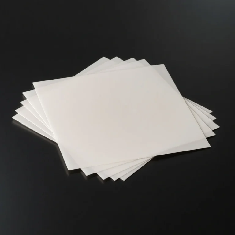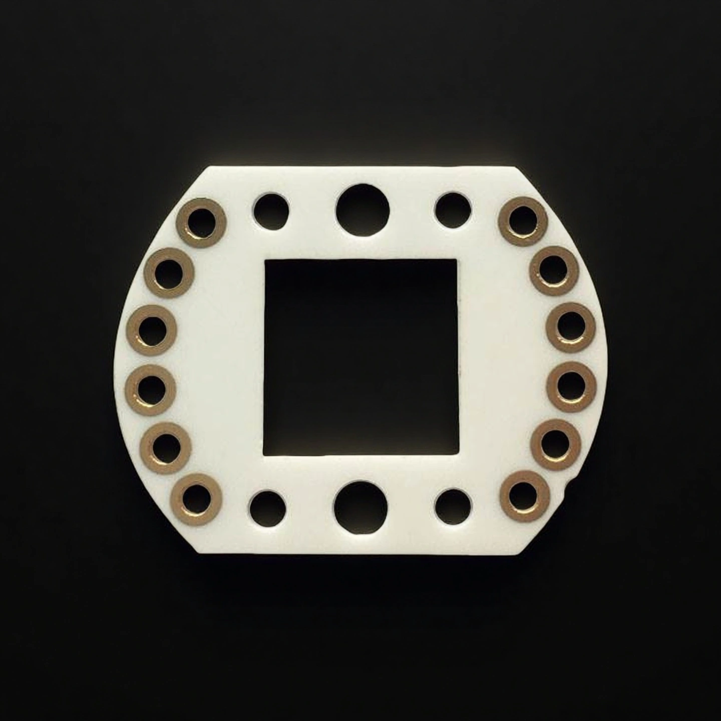
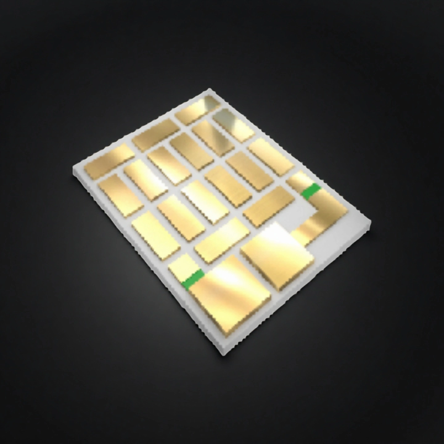
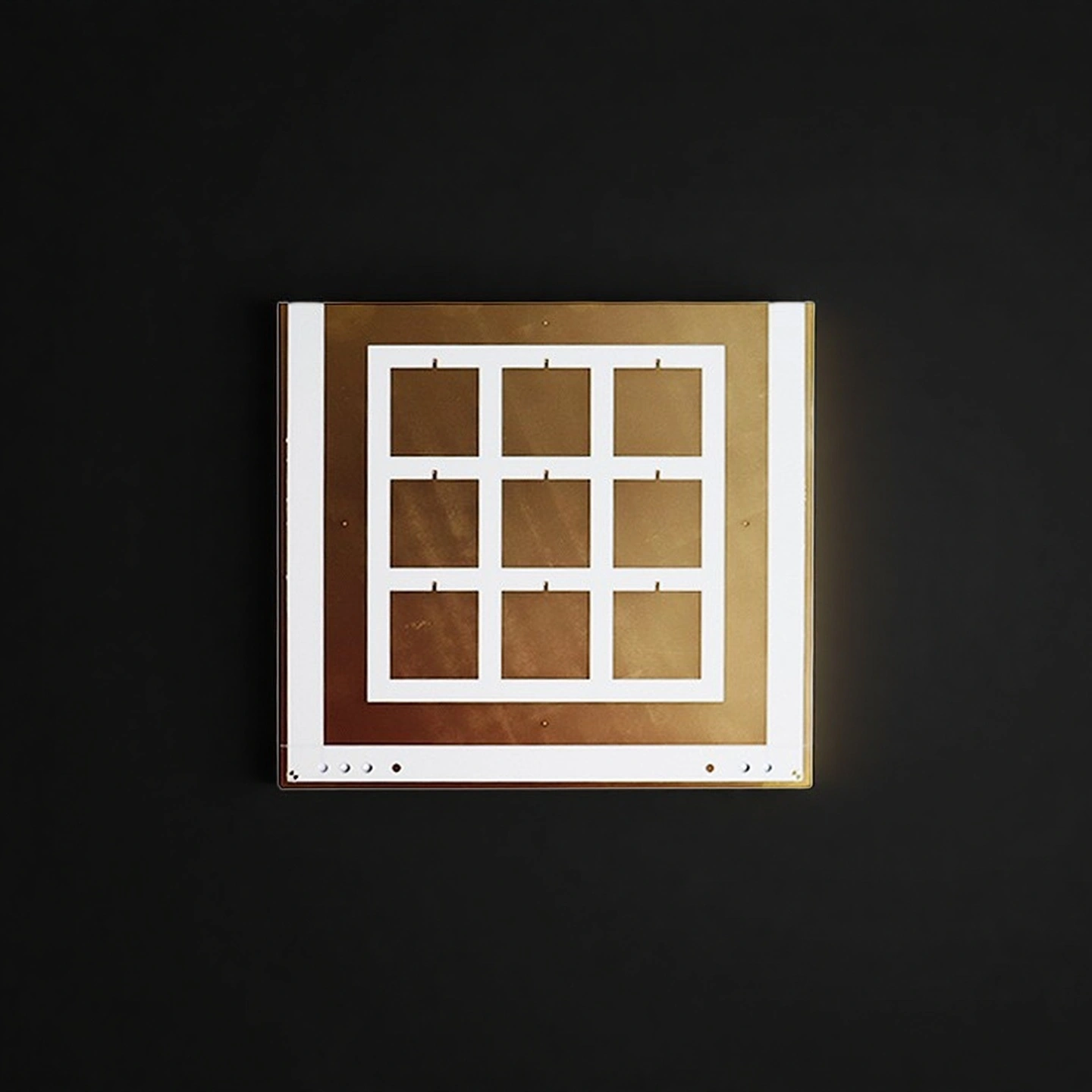
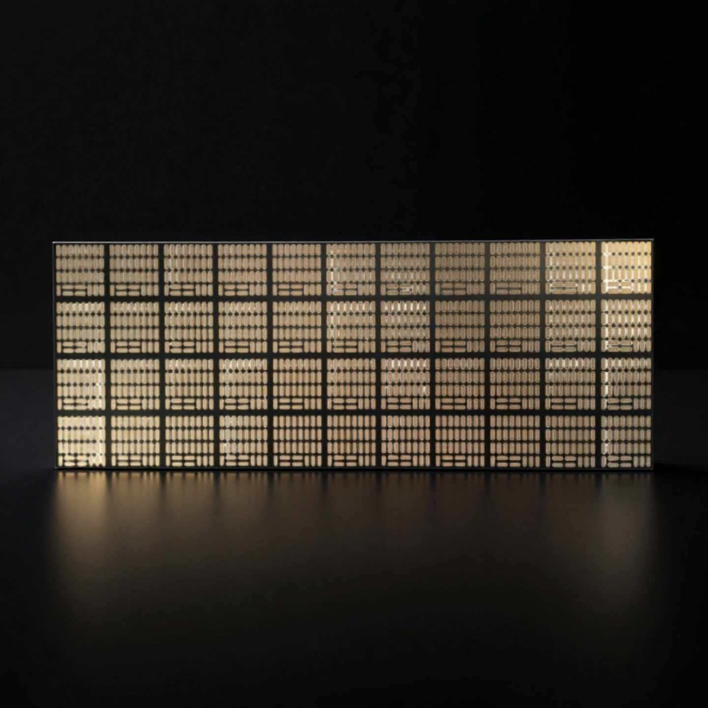
Metalized alumina substrate is a high-performance component used in electronics, as a small, flat tile made of alumina ceramic—a very hard, white material that is an excellent electrical insulator but also conducts heat well—onto which a thin layer of metal, usually copper, is bonded in a specific pattern, similar to the printed wires on a traditional circuit board.
Alumina Metalized Ceramic Substrate Benefits
- Exceptional Thermal Dissipation: Constructed from 96% or 99.6% purity alumina (Al₂O₃), our substrates conduct heat away from critical components like IGBTs and LEDs, preventing thermal failure and extending device lifespan.
- Stable Electrical Performance: The high dielectric strength and low dielectric loss of alumina ensure reliable electrical isolation at high voltages and maintain signal integrity in high-frequency RF applications.
- Strong Metallization Adhesion: Utilizing advanced metallization processes (DBC, DPC, Thick Film), the copper and refractory metal layers form a permanent bond with the ceramic, withstanding severe thermal cycling and mechanical stress without delamination.
- Precision Patterning: Laser processing and photolithography enable circuit trace and space resolution down to 30μm, facilitating the design of dense and complex electronic modules
Metalized Alumina Substrate Properties
| Property | Unit | 96% Al₂O₃ | 99% Al₂O₃ | 99.5% Al₂O₃ | 99.6% Al₂O₃ | 99.7% Al₂O₃ | 99.8% Al₂O₃ | 99.9% Al₂O₃ | 99.99% Al₂O₃ |
| Alumina content | % | 96 | 99 | 99.5 | 99.6 | 99.7 | 99.8 | 99.9 | 99.99 |
| Density | g/cm³ | 3.6-3.75 | 3.83 | 3.89 | 3.91 | 3.92 | 3.93 | 3.94 | 3.98 |
| Color | – | white | Ivory | Ivory | Ivory | Ivory | Ivory | Ivory | Ivory |
| Water absorption | % | 0 | 0 | – | 0 | 0 | 0 | 0 | 0 |
| Young’s modulus (Elastic modulus) | GPa | 300 | 350 | 375 | 356 | 357 | 358 | 359 | 362 |
| Shear modulus | GPa | – | – | 152 | – | – | – | – | – |
| Bulk modulus | GPa | – | – | 228 | – | – | – | – | – |
| Poisson’s ratio | – | – | – | 0.22 | – | – | – | – | – |
| Compressive strength | MPa | 1910 | 2210 | 2600 | 2552 | 2554 | 2556 | 2558 | 2570 |
| Flexural strength | MPa | 260 | 300 | 379 | 312 | 313 | 314 | 315 | 320 |
| Fracture toughness | MPa·m¹ᐟ² | – | – | 4 | – | – | – | – | – |
| Hardness | GPa | 14.5 | 17 | 17 | 23 | 24 | 25 | 26 | 30 |
| Thermal conductivity | W/m·K | 22 | 24 | 35 | 32–37 | 33–38 | 34–39 | 35–40 | 36–42 |
| Thermal shock resistance ΔT | °C | – | – | – | 222 | 223 | 224 | 225 | 228 |
| Maximum use temperature (no load) | °C | 1450 | 1680 | ≤1750 | 1755 | 1760 | 1765 | 1770 | 1800 |
| Coefficient of thermal expansion | 10⁻⁶/°C | 7.6 | 7.6 | 8.4 | – | – | – | – | – |
| Volume resistivity | Ω·cm | >1×10¹⁴ | >1×10¹⁴ | >1×10¹⁴ | >1×10¹⁴ | >1×10¹⁴ | >1×10¹⁴ | >1×10¹⁴ | >1×10¹⁴ |
| Dielectric constant (relative permittivity) | – | 9.2 | 9.5 | 9.8 | 9.83 | 9.84 | 9.85 | 9.86 | 9.92 |
| Dielectric strength | kV/mm | 15 | 19 | 16.9 | 23.2 | 23.4 | 23.6 | 23.8 | 24 |
| Dissipation factor (loss factor @ 1 kHz) | – | – | – | 0.0002 | – | – | – | – | – |
Al2O3 Metalized Ceramic Substrate Specifications
Type 1: Rectangle Alumina Metalized Ceramic Substrate

| Rectangle Alumina Metalized Ceramic Substrate | ||||||
| Item No. | Length(mm) | Width(mm) | Thickness(mm) | Copper foil thickness (mm) | Copper clad thickness(mm) | Purity(%) |
| AT-DBC-C001 | 10 | 5 | 0.25 | 0.1-0.6 | 0.075-0.1 | 96-99.7 |
| AT-DBC-C002 | 18 | 11 | 0.25 | 0.1-0.6 | 0.075-0.1 | 96-99.7 |
| AT-DBC-C003 | 20 | 15 | 0.38 | 0.1-0.6 | 0.075-0.1 | 96-99.7 |
| AT-DBC-C004 | 28 | 9 | 0.635 | 0.1-0.6 | 0.075-0.1 | 96-99.7 |
| AT-DBC-C005 | 32 | 24 | 0.55 | 0.1-0.6 | 0.075-0.1 | 96-99.7 |
| AT-DBC-C006 | 55 | 30 | 6 | 0.1-0.6 | 0.035 | 96 |
| AT-DBC-C007 | 70 | 52 | 0.76 | 0.1-0.6 | 0.075-0.1 | 96-99.7 |
| AT-DBC-C008 | 84 | 35 | 1 | 0.1-0.6 | 0.075-0.1 | 96-99.7 |
| AT-DBC-C009 | 103 | 90 | 0.635 | 0.1-0.6 | 0.075-0.1 | 96-99.7 |
| AT-DBC-C010 | 127 | 105 | 2 | 0.1-0.6 | 0.075-0.1 | 96-99.7 |
| AT-DBC-C011 | 156 | 84 | 3 | 0.1-0.6 | 0.075-0.1 | 96-99.7 |
| AT-DBC-C012 | 178 | 138 | 5 | 0.1-0.6 | 0.075-0.1 | 96-99.7 |
| AT-DBC-C013 | 188 | 138 | 4.6 | 0.1-0.6 | 0.075-0.1 | 96-99.7 |
Type 2: Square Alumina Metalized Ceramic Substrate
| Square Alumina Metalized Ceramic Substrate | ||||||
| Item No. | Length(mm) | Width(mm) | Thickness(mm) | Copper foil thickness (mm) | Copper clad thickness(mm) | Purity(%) |
| AT-DBC-Z001 | 10 | 10 | 0.25 | 0.1-0.6 | 0.075-0.1 | 96-99.7 |
| AT-DBC-Z002 | 15 | 15 | 0.25 | 0.1-0.6 | 0.075-0.1 | 96-99.7 |
| AT-DBC-Z003 | 18 | 18 | 0.25 | 0.1-0.6 | 0.075-0.1 | 96-99.7 |
| AT-DBC-Z004 | 25 | 25 | 0.38 | 0.1-0.6 | 0.075-0.1 | 96-99.7 |
| AT-DBC-Z005 | 31.5 | 31.5 | 0.635 | 0.1-0.6 | 0.075-0.1 | 96-99.7 |
| AT-DBC-Z006 | 33 | 33 | 0.76 | 0.1-0.6 | 0.075-0.1 | 96-99.7 |
| AT-DBC-Z007 | 40 | 40 | 0.76 | 0.1-0.6 | 0.075-0.1 | 96-99.7 |
| AT-DBC-Z008 | 60 | 60 | 1 | 0.1-0.6 | 0.075-0.1 | 96-99.7 |
| AT-DBC-Z009 | 72 | 72 | 1 | 0.1-0.6 | 0.075-0.1 | 96-99.7 |
| AT-DBC-Z010 | 100 | 100 | 3 | 0.1-0.6 | 0.075-0.1 | 96-99.7 |
| AT-DBC-Z011 | 127 | 127 | 1 | 0.1-0.6 | 0.035 | 99.7 |
| AT-DBC-Z012 | 138 | 138 | 5 | 0.1-0.6 | 0.075-0.1 | 96-99.7 |
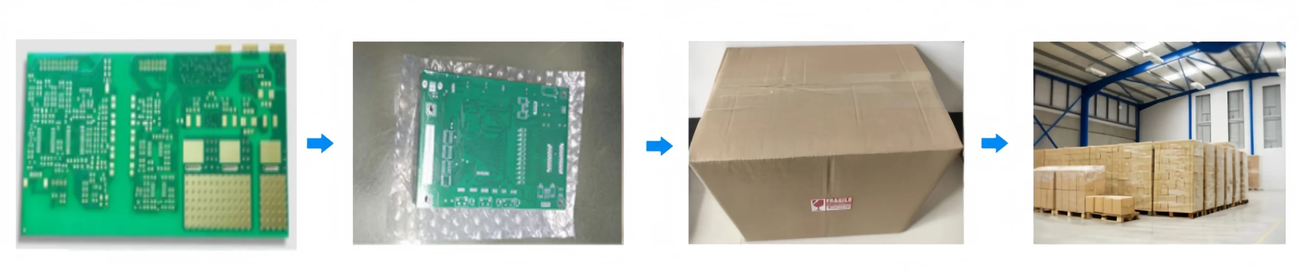
Metalized Alumina Substrate Packaging
- Each metalized ceramic part is sealed, packed, and placed in anti-static trays with moisture-proof bags. Shock-resistant outer cartons ensure integrity during transport.