What Is a Silicon Carbide Substrate?
A silicon carbide substrate is a flat SiC ceramic or crystal-based support material used in high-power, high-frequency, high-temperature and thermal management applications. Compared with many conventional ceramic substrates, SiC offers a strong combination of thermal conductivity, electrical stability, low thermal expansion, hardness and chemical resistance.
For engineering buyers, the key selection factors are not only the material name, but also the substrate type, conductivity level, crystal orientation, thickness, flatness, surface roughness, hole design, edge condition and packaging requirement. ADCERAX® supports custom SiC substrate supply for prototype development, equipment integration and application-specific ceramic component projects.
Advanced Material Characteristics of Silicon Carbide Substrates
Silicon carbide substrates are selected when thermal, electrical and mechanical requirements must be balanced in the same base material. The following characteristics help engineers evaluate whether SiC is suitable for power modules, RF platforms, high-temperature sensors and custom thermal management assemblies.
● Wide Bandgap and High Breakdown Strength
SiC has a wide bandgap and strong breakdown field capability, making it suitable for high-voltage, high-temperature and high-frequency designs. These properties are important when the substrate must support compact module structures and stable electrical behavior under demanding operating conditions.
● Efficient Heat Spreading
The high thermal conductivity of silicon carbide helps move heat away from active device areas, bonding interfaces or thermal contact surfaces. This is especially valuable in power electronics, RF modules, laser systems and high-temperature assemblies where local heat buildup may affect performance stability.
● Low Thermal Expansion
SiC has relatively low thermal expansion, which helps reduce stress during heating, cooling and repeated temperature transitions. This property is useful when the substrate is bonded, coated, metallized or assembled with other materials that may expand at different rates.
● Mechanical Stiffness and Surface Durability
The high elastic modulus and hardness of SiC help maintain dimensional stability during machining, mounting and operation. These properties also improve wear resistance, but they require careful control of edge processing, hole machining and surface handling.
● Conductive and Semi-Insulating Options
Silicon carbide substrates can be reviewed in conductive or semi-insulating forms according to the application. Conductive options are often considered for power-related structures, while semi-insulating options are more suitable for RF, microwave and isolation-sensitive platforms.
● Surface and Geometry Control
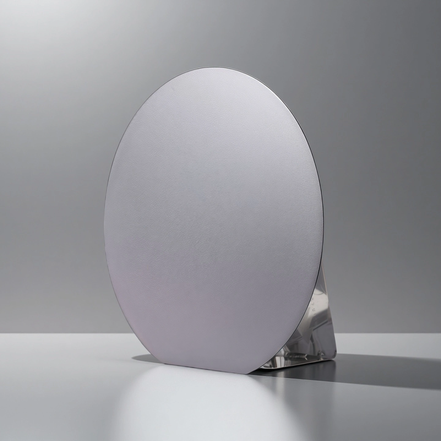
Surface finish, flatness, thickness, TTV, warp and edge condition are important for bonding, coating, thin-film deposition and precision assembly. For polished or application-specific substrates, these requirements should be confirmed according to the drawing, inspection method and downstream process.
● Chemical and Thermal Stability
SiC maintains strong stability in many high-temperature, corrosive and oxidizing environments. This makes it suitable for harsh industrial modules, thermal platforms, process fixtures and custom ceramic support structures where metals or conventional ceramics may not provide enough combined resistance.
Technical Specifications of Silicon Carbide Substrate
The Silicon Carbide Substrate exhibits quantifiable physical, thermal, electrical, and structural characteristics that define its behavior in high-temperature, high-frequency, and high-power applications, allowing consistent performance analysis in laboratory and device-development environments.
| Property | Specification | Application Relevance |
|---|---|---|
| Crystal Structure | Hexagonal (4H-SiC / 6H-SiC) | The hexagonal structure supports stable electrical, thermal and mechanical behavior in advanced device platforms. |
| Bandgap | 3.2–3.4 eV | The wide bandgap helps SiC substrates operate in high-voltage, high-temperature and high-frequency environments. |
| Breakdown Electric Field | ~3 MV/cm | A high breakdown field supports compact power device designs that require strong voltage endurance. |
| Thermal Conductivity | 120–160 W/m·K | High thermal conductivity helps transfer heat away from power modules, RF devices and thermal assemblies. |
| Coefficient of Thermal Expansion | 4.0–4.6 × 10⁻⁶ /K | Low thermal expansion helps reduce stress during heating, cooling and repeated thermal cycling. |
| Elastic Modulus | 450–470 GPa | High stiffness helps maintain dimensional stability during machining, mounting and device operation. |
| Hardness | Mohs ≈ 9 | High hardness improves wear resistance and surface durability, but it also requires precise machining and careful edge protection. |
| Resistivity Range (Semi-Insulating) | >10⁵ Ω·cm | High resistivity is important for RF, microwave and isolation-sensitive device structures. |
| Resistivity Range (Conductive) | n-type / p-type engineered windows | Conductive options allow engineers to match substrate behavior with power device or electrical integration requirements. |
| Surface Roughness (Epi-Ready) | <1 nm RMS | A very smooth surface supports bonding, thin-film deposition and epitaxial processing where interface quality is critical. |
| Micropipe Density | ppm-level | Lower defect density helps improve substrate consistency for demanding device and research applications. |
| Dielectric Constant | ~9.7 | Stable dielectric behavior supports RF, microwave and electrically sensitive module designs. |
| Refractive Index | 2.6–2.7 | Refractive behavior may matter in optical, photonic or sensor-related SiC substrate applications. |
| Thermal Shock Resistance | High stability under rapid cycling | Thermal shock resistance helps the substrate remain stable when exposed to fast temperature changes. |
| Chemical Resistance | Stable in acid, alkali and oxidizing media | Chemical resistance supports use in harsh processing, coating, high-temperature and corrosive environments. |
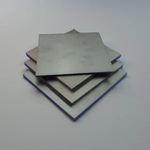
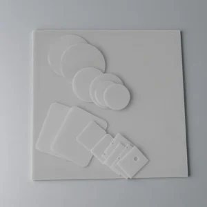
Silicon Carbide Substrate Crystal, Size and Processing Options
| SiC Substrate Specifications | |
|---|---|
| Growth Method | Seed Crystal Sublimation Method, PVT (Physical Vapor Transport) |
| Crystal Structure | Hexagonal |
| Lattice Constant | a=3.08 Å c=15.08 Å |
| Stacking Sequence | ABCACB |
| Orientation | Growth Axis or Off-axis <0001> 3.5° |
| Band Gap | 2.93 eV (Indirect) |
| Hardness | 9.2 (Mohs) |
| Thermal Conductivity @300K | 5 W/cm·K |
| Dielectric Constant | e(11)=e(22)=9.66 e(33)=10.33 |
| Dimensions | 10x3, 10x5, 10x10, 15x15, 20x15, 20x20, dia2", 15 x 15 mm, 10x10mm, etc. |
| Thickness | 0.5mm, 1.0mm |
| Polishing | Single-sided or Double-sided |
| Crystal Orientation | <001>±0.5° |
| Crystal Face Orientation Accuracy | ±0.5° |
| Edge Orientation Accuracy | 2° (Special requirements can reach within 1°) |
| Off-cut Wafer | Wafers with edge-oriented crystal faces can be processed at a specific angle (tilt angle 1° - 45°) according to specific requirements. |
| Ra: | ≤5Å (5μm×5μm) |
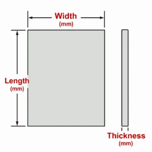
| Square Silicon Carbide Substrates | |||
| Item No. | Length(mm) | Width(mm) | Thickness (mm) |
| AT-SIC-CD001 | 10 | 3 | 0.5/1.0 |
| AT-SIC-CD002 | 10 | 5 | 0.5/1.0 |
| AT-SIC-CD003 | 10 | 10 | 0.5/1.0 |
| AT-SIC-CD004 | 15 | 15 | 0.5/1.0 |
| AT-SIC-CD005 | 20 | 15 | 0.5/1.0 |
| AT-SIC-CD006 | 20 | 20 | 0.5/1.0 |
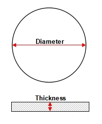
| Round Silicon Carbide Substrates | ||
| Item No. | Diameter(Inches) | Thickness (mm) |
| AT-SIC-CD101 | 2inches | 0.5/1.0 |
| AT-SIC-CD102 | 3inches | 0.5/1.0 |
| AT-SIC-CD103 | 4inches | 0.5/1.0 |
| AT-SIC-CD104 | 6inches | 0.5/1.0 |
| AT-SIC-CD105 | 8inches | 0.5/1.0 |
Silicon Carbide Substrate Options for Different Device Requirements
Different SiC substrate applications require different electrical and surface conditions. ADCERAX® reviews the intended device structure, operating temperature, voltage level, RF frequency range, bonding process and mechanical interface before recommending a suitable substrate configuration.
Conductive SiC Substrates
Conductive silicon carbide substrates are commonly considered when electrical conduction, high-voltage tolerance, thermal spreading and compact device architecture are important. They are often evaluated for power electronics, high-current modules, thermal test platforms and device development work where heat and electrical behavior must be controlled together.
Semi-Insulating SiC Substrates
Semi-insulating SiC substrates are selected when electrical isolation and low parasitic coupling are important. RF, microwave and GaN-on-SiC related platforms often require high resistivity, stable dielectric behavior and reliable heat dissipation to reduce signal drift under continuous operation.
Custom SiC Ceramic Substrate Blanks
For equipment builders and industrial OEMs, SiC ceramic substrate blanks can be customized by size, thickness, surface finish, edge profile, holes and mechanical interface. This option is suitable when the substrate functions as a thermal, structural or insulating support rather than a standard semiconductor wafer.
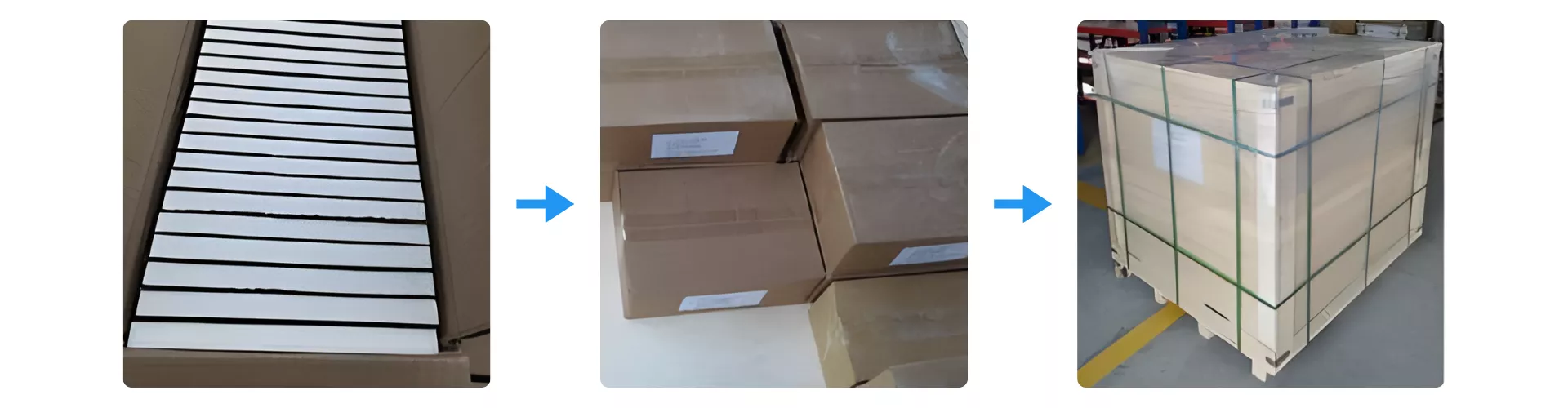
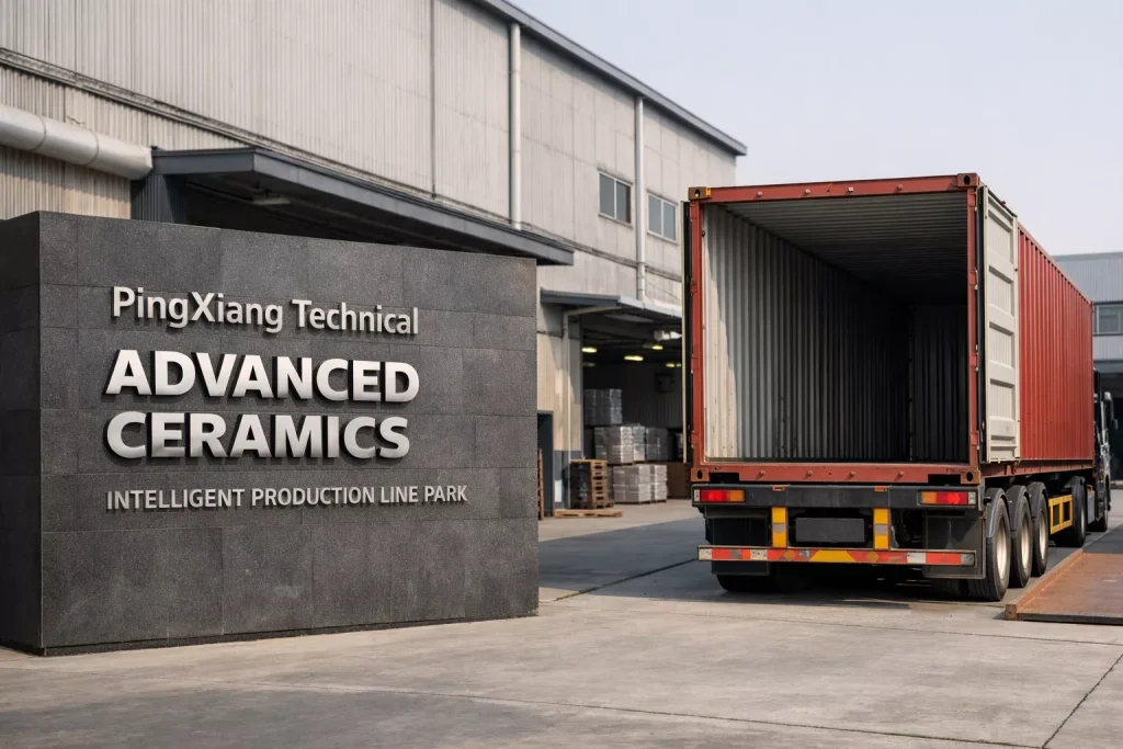
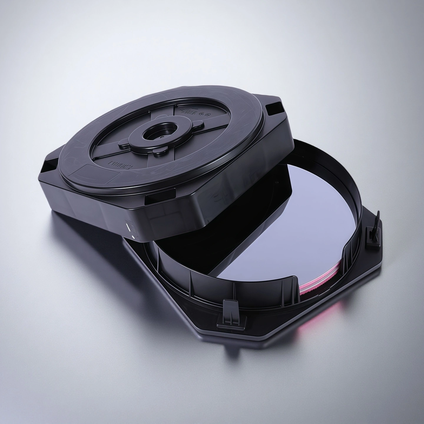
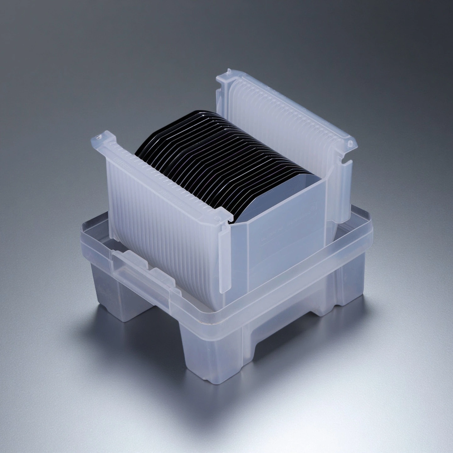
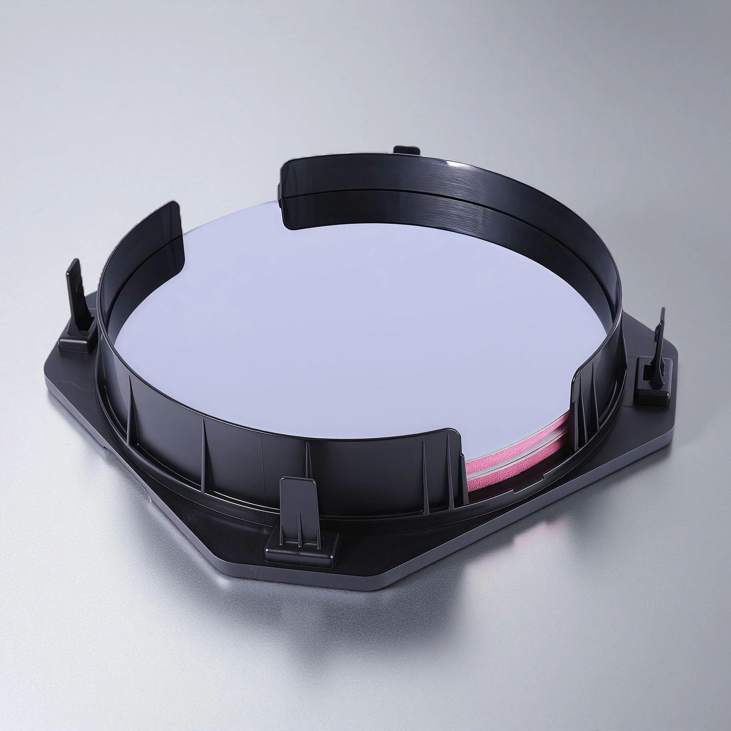
Protective Packaging for Silicon Carbide Substrate
Silicon Carbide Substrate is packed through a multi-stage protective system to ensure stability during long-distance transportation. Each substrate is first placed in individual reinforced cartons, which are then consolidated into labeled shipping boxes to maintain traceability. All boxed units are finally secured on palletized frames with full perimeter strapping to prevent vibration, compression, or impact throughout the global logistics process.