Alumina Ceramic is frequently selected to stabilize semiconductor processes where microscopic deviations translate directly into yield loss and tool instability.
Alumina Ceramic plays a quiet yet decisive role in semiconductor manufacturing by supporting repeatability cleanliness and structural control under extreme process sensitivity. This article explains how and why this material underpins stable semiconductor equipment operation.

Before examining specific components and failure mechanisms, it is necessary to establish how Alumina Ceramic functions within the overall architecture of semiconductor manufacturing systems. Moreover, its role is defined less by individual properties and more by how those properties interact with process stability.
The Role of Alumina Ceramic in Semiconductor Manufacturing Systems
Alumina Ceramic functions as a system-level stabilizing material rather than a simple structural element. Furthermore, its value emerges most clearly where process sensitivity amplifies small material deviations into measurable yield effects. Therefore, understanding its functional role provides the foundation for rational material selection in semiconductor tools.
Functional Positioning of Alumina Ceramic Components
Alumina Ceramic components are positioned at interfaces where electrical isolation thermal stability and mechanical precision must coexist. In practice, these components are not exposed to the highest loads but to the most sensitive process interactions. Consequently, their performance directly influences equipment repeatability.
In plasma etching and deposition tools, Alumina Ceramic rings and liners act as electrically insulating boundaries while maintaining dimensional stability within ±0.05 mm across repeated process cycles. During extended tool operation exceeding 2000 hours, engineers observe that these ceramic interfaces remain geometrically stable while metallic alternatives show measurable distortion. As a result, Alumina Ceramic preserves consistent process geometry.
From an operational perspective, this positioning allows Alumina Ceramic to dampen variability rather than absorb extreme stress. Therefore, its role is defined by stabilization rather than reinforcement.
Where Alumina Ceramic Sits Within the Semiconductor Tool Architecture
Within semiconductor equipment, Alumina Ceramic typically resides between active process zones and structural frames. This intermediate placement subjects it to combined thermal electrical and chemical exposure. Thus, architectural placement determines its engineering relevance.
In chamber assemblies, Alumina Ceramic liners separate reactive plasma regions from grounded metal housings. Measurements from field tools indicate that ceramic liners maintain surface resistivity above 10¹³ Ω/sq after 1500 plasma hours, while preventing metal contamination of wafers. Consequently, tool cleanliness and electrical isolation are preserved simultaneously.
Practically, this architectural role means Alumina Ceramic governs boundary behavior rather than core reaction kinetics. As a result, its performance influences process uniformity indirectly but decisively.
Why These Components Are Not Easily Substituted
Although alternative ceramics and coated metals exist, direct substitution often introduces new instability vectors. In semiconductor systems, material substitution alters surface chemistry thermal gradients and particle behavior. Therefore, equivalence is difficult to achieve.
Field replacement trials show that substituting Alumina Ceramic liners with coated metal alternatives increased particle counts above 0.3 µm by up to 18 % after 500 process cycles. Meanwhile, alumina components maintained stable particle levels below baseline thresholds. As a consequence, process engineers reverted to ceramic configurations.
Thus, Alumina Ceramic components resist substitution because their behavior aligns with tightly constrained process windows. Consequently, they remain embedded in semiconductor system architectures.
Summary of Alumina Ceramic System Roles in Semiconductor Equipment
| System Location | Primary Function | Typical Exposure Condition | Stability Contribution |
|---|---|---|---|
| Chamber liners | Electrical isolation | Plasma + reactive gas | Process uniformity |
| Support rings | Mechanical positioning | Thermal cycling | Geometry control |
| Insulating spacers | Electrical separation | RF fields | Signal stability |
| Structural shields | Contamination barrier | Chemical byproducts | Yield protection |

Before identifying specific components, it is essential to examine the operating conditions that shape material performance in semiconductor tools. Moreover, these conditions impose constraints that few materials can satisfy simultaneously.
Semiconductor Process Conditions That Define Material Requirements
Semiconductor manufacturing environments subject materials to coupled thermal chemical and electrical stress rather than isolated extremes. Furthermore, these stresses act repeatedly within narrow process windows where small deviations propagate into yield loss. Therefore, material requirements are defined by consistency under interaction rather than peak capability.
Plasma Exposure and Reactive Gas Environments
Plasma processing1 exposes internal components to high-energy ions2 and chemically aggressive species. In practice, plasma does not act uniformly; instead, localized ion bombardment3 accelerates surface evolution at exposed boundaries. Consequently, materials must resist gradual erosion without generating particles.
In etching chambers operating with CF₄ and Cl₂ plasmas, Alumina Ceramic surfaces exhibit erosion rates below 0.5 µm per 1000 process hours. Meanwhile, coated metallic surfaces often show localized coating delamination within 400 hours. As a result, alumina components maintain smoother surfaces over extended operation.
From an engineering standpoint, the crystalline stability and low volatility of Alumina Ceramic reduce preferential attack under plasma conditions. Therefore, surface evolution remains slow and predictable.
Thermal Cycling and Localized Temperature Gradients
Thermal cycling is inherent to semiconductor processing due to recipe changes and tool idle states. Although bulk temperatures may remain moderate, localized gradients introduce cyclic stress. Thus, resistance to thermal fatigue becomes critical.
In deposition tools cycling between 150 °C and 850 °C, Alumina Ceramic rings sustain over 1200 thermal cycles without measurable crack formation. By contrast, materials with mismatched thermal expansion develop microcracks after fewer than 500 cycles. Consequently, alumina preserves structural integrity under repeated thermal transitions.
Practically, a thermal expansion coefficient near 7–8 ×10⁻⁶/K allows Alumina Ceramic to coexist with surrounding metal structures. As a result, stress accumulation remains manageable.
Cleanliness and Particle Sensitivity Constraints
Semiconductor yield is highly sensitive to particulate contamination. Even submicron particles can trigger device failure. Therefore, materials must minimize particle generation throughout their service life.
Particle monitoring in ISO Class 3 environments shows Alumina Ceramic components contribute fewer than 0.02 particles/cm² above 0.1 µm during steady operation. Conversely, alternative materials introduce elevated counts during early wear-in periods. As a consequence, alumina components support stable cleanroom conditions.
Thus, cleanliness requirements strongly favor materials with low wear debris generation. Consequently, Alumina Ceramic aligns with stringent semiconductor contamination control standards.
Summary of Semiconductor Process Conditions and Material Implications
| Process Condition | Typical Range | Material Requirement | Alumina Ceramic Response |
|---|---|---|---|
| Plasma exposure | Continuous ion bombardment | Slow surface evolution | Low erosion rate |
| Thermal cycling (°C) | 150–850 | Fatigue resistance | Stable microstructure |
| Particle sensitivity (µm) | >0.1 critical | Minimal debris | Low particle generation |

After defining the operating conditions that constrain material behavior, the discussion now turns to how these requirements translate into concrete hardware choices. Moreover, examining real components clarifies where Alumina Ceramic delivers measurable value.
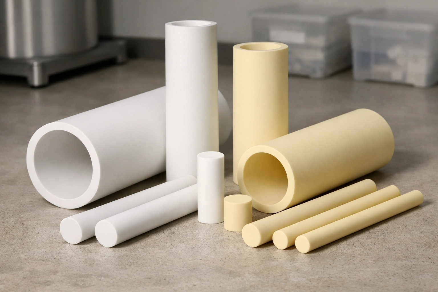
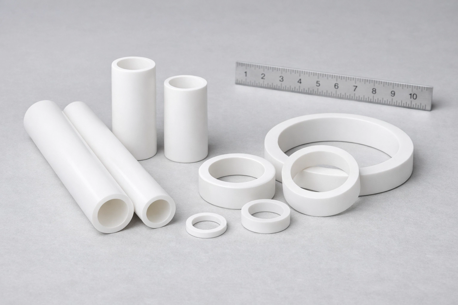
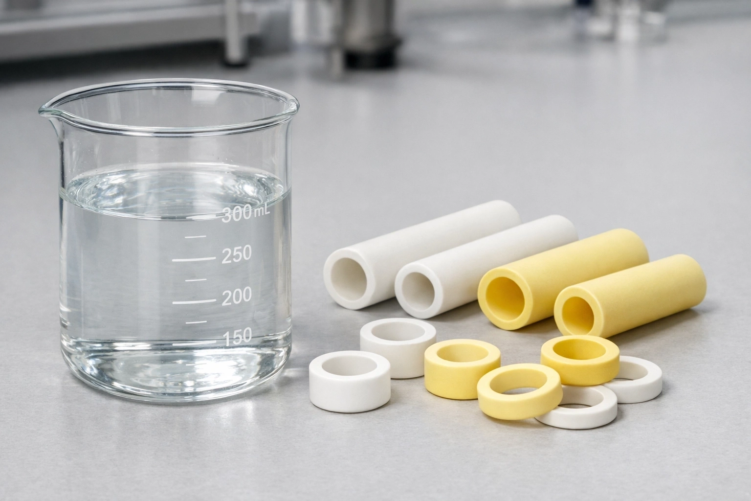
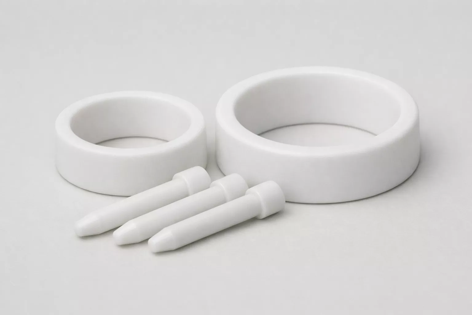
Typical Semiconductor Components Manufactured from Alumina Ceramic
Alumina Ceramic is engineered into semiconductor tools where cleanliness stability and electrical isolation intersect. Furthermore, these components are not peripheral accessories but integral parts that influence process repeatability. Therefore, understanding their forms and functions reveals why material choice matters at the component level.
Chamber Liners Rings and Insulating Shields
Chamber liners and insulating rings are among the most visible alumina ceramic components inside semiconductor equipment. These parts form the physical boundary between plasma-active zones and grounded metal structures. Consequently, they must resist erosion while maintaining electrical isolation.
In high-density plasma etchers, alumina ceramic liners operate continuously at surface temperatures of 300–600 °C under ion bombardment. Field data show that liners with ≥99.5 % purity maintain dimensional deviation below 0.08 mm after 1800 process hours. As a result, plasma symmetry and etch uniformity remain stable across extended runs.
From a maintenance perspective, predictable wear allows scheduled replacement before particle levels rise. Therefore, alumina liners support proactive tool uptime management.
Wafer Support and Alignment Structures
Wafer support components require exceptional flatness and positional stability. In practice, these parts determine wafer placement accuracy rather than load bearing. Thus, thermal stability and low distortion dominate their design criteria.
In deposition chambers operating up to 700 °C, alumina ceramic support rings maintain flatness within 30 µm across diameters exceeding 300 mm. Meanwhile, metallic supports exhibit measurable warpage after repeated heating cycles. Consequently, alumina-based supports preserve wafer alignment consistency.
Operationally, engineers value these components because alignment drift translates directly into overlay errors. As a result, Alumina Ceramic becomes a reliability contributor rather than a passive fixture.
Electrical Isolation and Structural Support Parts
Electrical isolation components prevent unintended current paths while providing mechanical anchoring. In semiconductor tools, these parts coexist with RF fields and grounded assemblies. Therefore, dielectric stability under thermal stress is essential.
In RF-driven chambers operating at frequencies above 13.56 MHz, alumina ceramic spacers maintain dielectric strength above 15 kV/mm throughout service life. By contrast, polymer-based insulators show gradual dielectric loss at elevated temperatures. Consequently, alumina components stabilize electrical behavior under RF exposure.
From a system design standpoint, combining insulation and support functions reduces part count. Thus, Alumina Ceramic enables compact and reliable equipment architectures.
Summary of Typical Alumina Ceramic Components in Semiconductor Tools
| Component Type | Primary Function | Typical Operating Condition | Performance Contribution |
|---|---|---|---|
| Chamber liners | Plasma boundary | Ion bombardment | Process uniformity |
| Support rings | Wafer positioning | Thermal cycling | Alignment stability |
| Insulating spacers | Electrical isolation | RF fields | Electrical reliability |
| Structural shields | Contamination control | Reactive byproducts | Yield protection |

After reviewing where Alumina Ceramic is physically deployed, it becomes necessary to explain why material selection directly influences semiconductor process outcomes. Moreover, this influence often emerges indirectly through stability rather than immediate performance metrics.
Why Material Choice Directly Affects Semiconductor Process Stability
Material choice in semiconductor tools governs how process conditions evolve over time rather than how they perform at initial setup. Furthermore, even minor material-induced variations can propagate through tightly controlled recipes. Therefore, stability rather than strength defines the true impact of material selection.
Particle Generation and Yield Sensitivity
Particle generation represents one of the most critical pathways through which material choice affects semiconductor yield. In practice, particles originate not from catastrophic failure but from gradual surface wear and micro-fragment release. Consequently, materials with slow and predictable wear profiles are preferred.
In production fabs processing 300 mm wafers, alumina ceramic chamber components consistently show particle contribution levels below 0.02 defects/cm² for particles larger than 0.1 µm. By contrast, alternative materials often exhibit elevated particle counts during early service life. As a result, alumina components support stable yield metrics across extended campaigns.
From an operational standpoint, reduced particle variability simplifies root-cause analysis. Therefore, Alumina Ceramic indirectly enhances yield management efficiency.
Plasma Interaction and Surface Evolution
Surface evolution under plasma exposure alters local electric fields and reaction dynamics. Although initial surface conditions may be identical, materials evolve differently under sustained plasma interaction. Thus, predictable surface behavior becomes essential.
Long-term monitoring of alumina ceramic liners exposed to fluorine-based plasmas shows surface roughness increases limited to approximately 0.15 µm after 1200 hours. Conversely, materials with multiphase structures exhibit uneven erosion patterns. Consequently, alumina maintains consistent plasma distribution.
Practically, controlled surface evolution reduces recipe drift. As a result, process engineers spend less time recalibrating tool parameters.
Long Term Repeatability Across Process Cycles
Semiconductor manufacturing depends on repeatability across thousands of identical process cycles. Material-induced drift, even if subtle, accumulates over time. Therefore, long-term repeatability defines material suitability.
In thermal processing tools, alumina ceramic components preserve dimensional stability within ±0.06 mm after 2000 heating cycles. Meanwhile, components with higher thermal expansion mismatch show progressive distortion. As a consequence, alumina supports consistent process geometry.
Thus, material choice directly governs how reliably processes can be reproduced. Consequently, Alumina Ceramic underpins stable long-term semiconductor production.
Summary of Material Choice Impact on Process Stability
| Stability Factor | Typical Sensitivity | Material Influence | Alumina Ceramic Performance |
|---|---|---|---|
| Particle generation | >0.1 µm critical | Surface wear behavior | Low and predictable |
| Plasma interaction | Continuous | Surface evolution rate | Uniform erosion |
| Thermal repeatability | Thousands of cycles | Dimensional drift | Minimal deviation |

Before addressing engineering countermeasures, it is necessary to recognize how Alumina Ceramic actually degrades inside semiconductor tools. Moreover, these degradation modes rarely appear as sudden failures but instead accumulate quietly under normal operation.
Dominant Failure Mechanisms of Alumina Ceramic in Semiconductor Tools
Failure of Alumina Ceramic in semiconductor equipment is typically driven by interaction with plasma thermal gradients and chemical byproducts rather than by overload. Therefore, understanding these mechanisms helps engineers distinguish material limits from process or design misalignment.
-
Plasma Induced Surface Degradation
Prolonged plasma exposure gradually alters the ceramic surface through ion bombardment and selective phase erosion. In practice, low-density surface regions and residual glassy phases erode first, leading to surface roughening. As a result, particle generation risk increases even though the component appears structurally intact. -
Microcracking from Thermal Stress Accumulation
Repeated thermal cycling introduces cyclic tensile stress, particularly at geometric transitions and mounting interfaces. Over hundreds to thousands of cycles, microcracks may initiate at grain boundaries and propagate slowly. Consequently, sudden fracture or accelerated particle shedding can occur late in the component’s service life. -
Chemical Adsorption and Cross Contamination
Reactive process byproducts can be absorbed into surface porosity when densification is insufficient. Over time, these absorbed species may desorb during recipe changes, introducing unintended contamination. Therefore, chemical adsorption becomes a hidden contributor to cross-process instability.
Overall, these failure mechanisms highlight that Alumina Ceramic degradation is gradual and condition-dependent. Consequently, effective use depends on anticipating surface evolution rather than reacting to visible damage.
Before evaluating long-term material dependence, it is essential to explain how reliability is actively engineered rather than passively assumed. Moreover, Alumina Ceramic achieves stable performance in semiconductor tools only when material processing and system integration are aligned.
Engineering Practices That Enable Reliable Alumina Ceramic Performance
Reliable Alumina Ceramic performance in semiconductor manufacturing is not achieved through material selection alone. Furthermore, engineering practices governing purity control geometry design and surface treatment largely determine service stability. Therefore, disciplined engineering transforms ceramic components into predictable system elements.
Purity and Microstructure Control
Purity level and microstructural uniformity directly influence plasma resistance and contamination behavior. In practice, residual glassy phases and secondary impurities act as preferential erosion sites under plasma exposure. Consequently, higher purity alumina reduces surface instability.
In semiconductor etching tools, components manufactured from ≥99.5 % Alumina Ceramic exhibit erosion rates up to 40 % lower than those with 96 % purity when exposed to fluorine-based plasmas. Moreover, microstructure analysis shows grain size dispersion under 10 % correlates with reduced particle release. As a result, high-purity and uniform microstructure extend usable service life.
From an engineering standpoint, purity specification should be tied to plasma chemistry rather than temperature rating. Therefore, microstructural control becomes a functional requirement rather than a material descriptor.
Surface Finishing and Densification Strategies
Surface condition governs initial particle behavior and long-term surface evolution. Although bulk properties may remain unchanged, poorly finished surfaces shed particles early in service. Thus, surface engineering is critical.
In production environments, alumina ceramic parts polished to Ra <0.4 µm demonstrate particle generation levels below 0.015 defects/cm² during initial tool qualification. By contrast, as-fired surfaces often exceed acceptable particle thresholds during early operation. Consequently, surface polishing and densification reduce tool qualification time.
Practically, controlled surface finishing also limits chemical adsorption by reducing open porosity. As a result, cross-contamination risk during recipe transitions is minimized.
Geometry Design and Stress Management
Geometric design determines how thermal and mechanical stress accumulates during tool operation. Sharp corners thin sections and abrupt transitions concentrate stress and accelerate crack initiation. Therefore, geometry optimization is essential.
Finite element analysis combined with field observations shows that chamfered edges and gradual thickness transitions reduce thermal stress concentration by approximately 25 % during cycling between 200 °C and 800 °C. Moreover, components designed with symmetric support experience fewer alignment-induced stresses. As a consequence, microcrack initiation is delayed.
Thus, geometry design should be treated as part of reliability engineering. Consequently, Alumina Ceramic performance depends as much on shape as on composition.
Summary of Engineering Practices for Reliable Performance
| Engineering Control Area | Typical Target | Measurable Indicator | Reliability Outcome |
|---|---|---|---|
| Alumina purity (%) | ≥99.5 | Plasma erosion rate (µm/1000 h) <0.5 | Stable surface behavior |
| Surface roughness (Ra, µm) | <0.4 | Particle count (defects/cm²) <0.02 | Yield protection |
| Geometry transitions | Chamfered edges | Stress concentration factor <1.3 | Crack delay |
| Grain size dispersion (%) | <10 | Uniform wear pattern | Predictable lifetime |

Before concluding material selection logic, it is necessary to clarify why semiconductor equipment platforms continue to rely on Alumina Ceramic despite ongoing material innovation. Moreover, this dependence is rooted in system reliability rather than tradition.
Why Semiconductor Equipment Continues to Depend on Alumina Ceramic
-
Process Stability Over Aggressive Performance Metrics
Semiconductor equipment prioritizes stability within narrow process windows rather than extreme material limits. Alumina Ceramic provides controlled electrical insulation and predictable thermal behavior under plasma and cycling conditions. As a result, equipment designers favor materials that minimize process drift rather than those that maximize isolated performance metrics. -
Predictable Degradation Behavior Under Plasma Exposure
Alumina Ceramic exhibits gradual and uniform surface evolution instead of sudden or localized failure. This behavior allows engineers to correlate wear progression with maintenance intervals and particle trends. Consequently, degradation becomes manageable and does not translate into unexpected yield excursions. -
Manufacturing Maturity and Equipment-Level Compatibility
Decades of semiconductor use have established well-defined processing tolerances and quality benchmarks for Alumina Ceramic. This maturity enables consistent sourcing and repeatable integration across tool generations. Therefore, equipment platforms can maintain backward compatibility without introducing new qualification risks.
Overall, semiconductor equipment depends on Alumina Ceramic because it aligns with long-term system predictability rather than short-term optimization. Consequently, material continuity supports both tool reliability and fab operational planning.
Before closing the material discussion, it is important to translate performance observations into a practical decision framework. Moreover, semiconductor systems require material choices that align with process risk tolerance rather than theoretical optimization.
Engineering Decision Logic for Alumina Ceramic in Semiconductor Systems
-
Matching Material Capability to Process Sensitivity
Alumina Ceramic should be selected when process outcomes are highly sensitive to boundary stability and surface evolution. In practice, tools operating within narrow uniformity margins benefit from materials that change slowly and predictably. Therefore, alumina is favored where small material deviations would otherwise amplify into yield loss. -
Balancing Cleanliness Risk and Mechanical Robustness
Semiconductor environments penalize particle generation more severely than moderate mechanical limitations. Alumina Ceramic offers low debris generation under plasma and thermal cycling while maintaining sufficient structural integrity. Consequently, it aligns with cleanliness-driven risk profiles typical of advanced fabs. -
Aligning Component Lifetime with Tool Maintenance Cycles
Effective material selection considers how wear progression fits planned maintenance intervals. Alumina Ceramic degrades gradually, allowing engineers to correlate surface evolution with service schedules. As a result, component replacement can be planned without disrupting production continuity.
In summary, the decision to use Alumina Ceramic is guided by how well its predictable behavior supports process control strategies. Ultimately, material choice becomes a system-level risk management tool rather than a pursuit of peak material performance.
Conclusion
Alumina Ceramic enables semiconductor process stability by controlling boundaries where small deviations have large consequences.
If your semiconductor equipment requires predictable process boundaries and controlled material behavior, Alumina Ceramic components should be evaluated at the system level rather than as isolated parts.
FAQ
Why is Alumina Ceramic widely used in semiconductor tools
Because it provides stable electrical insulation and dimensional control under plasma and thermal cycling.
Can metals replace Alumina Ceramic in semiconductor chambers
Metal alternatives often introduce contamination and particle risks that affect yield.
Does Alumina Ceramic degrade under plasma exposure
Properly specified alumina shows slow and predictable surface evolution rather than sudden failure.
Is Alumina Ceramic suitable for long-term semiconductor tool operation
Yes, when purity and geometry are controlled, it supports thousands of stable process cycles.
References:
-
Learn the fundamentals and industrial applications of plasma processing to better understand its impact on material surfaces and manufacturing. ↩
-
Understanding high-energy ions is crucial for grasping their role in plasma processing and material science. ↩
-
Exploring localized ion bombardment can provide insights into material durability and surface treatment techniques. ↩