Alumina Substrate thickness is often selected too late in design cycles; consequently, hidden electrical and mechanical risks emerge. Therefore, early thickness decisions directly influence reliability margins, thermal behavior, and long-term manufacturing stability.
Alumina Substrate thickness selection directly shapes electrical insulation performance, thermal resistance, and mechanical integrity across power electronics, sensors, and industrial systems. This article provides an engineering-centered framework that aligns thickness decisions with real operating conditions, manufacturing constraints, and long-term reliability targets.

Before examining industry-specific thickness strategies, it is necessary to clarify why thickness should be treated as a core engineering variable rather than a dimensional afterthought.
Alumina Substrate Thickness as Engineering Variable
Thickness in an Alumina Substrate functions as an integrated engineering variable that simultaneously influences electrical safety, thermal behavior, and mechanical stability. Consequently, thickness selection should be evaluated at the same design priority level as material purity or surface finish.
-
Thickness influences electrical insulation margins beyond nominal dielectric ratings.
In practice, designers often observe that increasing substrate thickness by 20–30% can significantly reduce localized electric field intensity under high-voltage operation. As a result, thickness becomes a controllable lever for improving insulation robustness without changing material composition. -
Thickness governs thermal mass and temperature response behavior.
Thicker Alumina Substrate sections increase thermal inertia, which stabilizes temperature gradients during steady-state operation. However, thinner substrates reduce thermal mass and accelerate response speed, which can be advantageous in sensor and heater applications when structural limits are respected. -
Thickness defines mechanical stiffness and deformation resistance.
Mechanical bending stiffness scales approximately with the cube of thickness, meaning that small thickness changes can lead to large differences in warpage and stress distribution. Therefore, thickness selection strongly affects flatness retention during firing, grinding, and subsequent thermal cycling.
Taken together, these effects indicate that Alumina Substrate thickness acts as a system-level design parameter rather than an isolated dimension. Accordingly, the following sections analyze how thickness interacts with electrical, thermal, and mechanical mechanisms in greater detail.
Thickness Driven Electrical Thermal Mechanical Coupling
Before engineers assign thickness values to an Alumina Substrate, it is essential to recognize how electrical, thermal, and mechanical behaviors evolve simultaneously rather than independently. Consequently, thickness decisions always involve coupled trade-offs, where optimizing one domain can amplify constraints in another. Therefore, this section establishes a unified engineering framework that explains how thickness governs multi-physics interactions across real operating conditions.
Electrical Insulation Behavior Across Thickness Ranges
Electrical insulation performance in an Alumina Substrate scales with thickness, yet the relationship is not linear in real systems.
At moderate voltages, increasing thickness primarily extends the effective dielectric path length. However, in high-voltage environments, engineers frequently observe that local electric field concentration, rather than bulk dielectric strength, becomes the dominant failure driver. For example, field simulations and breakdown testing show that increasing substrate thickness from 0.38 mm to 0.63 mm can reduce peak electric field intensity near conductor edges by 18–25%, even when material purity remains unchanged.
In practice, power electronics engineers often recall early prototype failures where thin substrates passed nominal dielectric tests but failed during extended voltage endurance runs. This discrepancy arises because thickness also influences field redistribution under thermal expansion and mechanical constraint. Consequently, thickness acts as a stabilizing factor that improves long-term electrical reliability, particularly in IGBT and SiC power modules operating above 600 V.
Ultimately, electrical insulation cannot be evaluated using thickness alone; however, thickness provides a controllable margin that mitigates field-driven degradation mechanisms when integrated into holistic design.
Thermal Resistance and Heat Flow Control
Thermal behavior is frequently cited as the primary motivation for reducing Alumina Substrate thickness, yet thermal advantages diminish rapidly beyond certain limits.
From a conduction standpoint, thermal resistance scales approximately linearly with thickness for a given material conductivity. For instance, reducing thickness from 1.0 mm to 0.5 mm lowers through-thickness thermal resistance by roughly 50%, assuming identical interface conditions. Nevertheless, system-level measurements consistently demonstrate that interface resistance and heat spreading dominate once substrate thickness drops below 0.4–0.5 mm.
In applied settings, engineers developing heater substrates or power modules often encounter diminishing returns when pushing thickness below 0.3 mm. Although thinner substrates reduce intrinsic thermal mass, they simultaneously increase temperature gradients and amplify mechanical stress under rapid heating. Consequently, local hot spots form more readily, which can offset theoretical thermal gains.
Therefore, effective thermal control depends on selecting a thickness that balances conduction efficiency with temperature uniformity and mechanical survivability, rather than pursuing minimum thickness values.
Mechanical Stiffness Warpage and Stress Formation
Mechanical stiffness is the most underestimated aspect of Alumina Substrate thickness selection, yet it strongly governs manufacturing yield and field reliability.
Bending stiffness increases approximately with the cube of thickness, meaning that increasing thickness from 0.5 mm to 0.8 mm can raise flexural rigidity by nearly 300%. As a result, thicker substrates exhibit significantly lower warpage during sintering, grinding, and thermal cycling. In contrast, thin substrates below 0.4 mm are far more susceptible to residual stress accumulation and elastic deformation.
Experienced manufacturing engineers often recall scenarios where ultra-thin substrates appeared flat after polishing but warped noticeably after metallization or solder reflow. This behavior occurs because thermal expansion mismatch between layers releases stored elastic energy once constraints are removed. Consequently, thickness serves as a mechanical buffer that stabilizes geometry across multiple process steps.
In long-term service, thicker substrates also demonstrate improved resistance to vibration-induced fatigue and thermal shock, particularly in industrial power and insulation applications where temperature swings exceed 150–200°C.
Coupled Engineering Outcomes Across Domains
Electrical, thermal, and mechanical effects cannot be separated when evaluating Alumina Substrate thickness.
Increasing thickness enhances electrical insulation margins and mechanical stiffness; however, it raises thermal resistance and thermal inertia. Conversely, reducing thickness improves thermal response but elevates risks related to warpage, stress concentration, and dielectric endurance. Therefore, thickness selection represents a multi-domain optimization problem, not a single-parameter adjustment.
Seasoned engineers often resolve this coupling by defining dominant failure modes first. For high-voltage power modules, electrical and mechanical stability typically outweigh thermal gains. In sensor and heater devices, thermal response may dominate, provided mechanical limits are respected. This prioritization approach enables thickness values that align with real-world performance targets rather than theoretical extremes.
Summary of Thickness Coupling Effects
| Thickness Range (mm) | Electrical Insulation Stability | Thermal Resistance Trend | Mechanical Stiffness Level | Typical Application Focus |
|---|---|---|---|---|
| 0.25–0.38 | Moderate, field-sensitive | Low, fast response | Low | Sensors, fast heaters |
| 0.38–0.63 | High, stable fields | Balanced | Medium | Power electronics, hybrids |
| 0.63–1.00 | Very high, robust margin | Higher thermal inertia | High | Industrial insulation |

Thickness Selection for Power Electronics Substrates
In power electronics systems, Alumina Substrate thickness directly determines whether electrical insulation margins, thermal stability, and mechanical reliability1 can coexist under continuous stress. Consequently, thickness selection in this domain is rarely driven by a single parameter. Instead, it reflects a prioritized balance shaped by voltage class, power density, and expected lifetime loading.
Thickness Effects on Dielectric Safety Margins
In power modules, thickness is one of the most reliable levers for increasing dielectric robustness without altering material chemistry.
At operating voltages above 600 V, field measurements and accelerated testing repeatedly show that thinner substrates concentrate electric fields at metallization edges and ceramic surface defects. For example, increasing thickness from 0.40 mm to 0.63 mm typically reduces edge field intensity by 20–30%, which directly delays partial discharge inception under repetitive switching conditions.
In real project reviews, power engineers often recount early-stage designs that passed short-term withstand tests but failed during extended DC bias or surge cycling. These failures were later traced to insufficient thickness margins that allowed micro-discharges to develop under combined thermal and mechanical loading. Consequently, thickness becomes a practical insurance layer that stabilizes insulation behavior throughout the module’s service life.
Therefore, dielectric safety in power electronics is rarely maximized by minimum thickness. Instead, it is achieved by selecting a thickness that tolerates field redistribution under thermal expansion and assembly constraint.
Thickness Influence on Thermal Cycling Reliability
Thermal cycling represents one of the most severe stressors for Alumina Substrate assemblies in power electronics.
Repeated temperature swings of 120–180°C induce cyclic strain between ceramic substrates and attached metallization layers. Thinner substrates flex more easily, which initially appears beneficial. However, this flexibility accelerates fatigue accumulation at interfaces, particularly in soldered or brazed joints. Empirical lifetime testing shows that substrates thinner than 0.38 mm may experience crack initiation 30–40% earlier than thicker counterparts under identical thermal cycling profiles.
By contrast, increasing thickness to 0.5–0.8 mm significantly improves stiffness and redistributes thermally induced stress across a larger volume. In practice, engineers observe fewer interfacial cracks and more predictable deformation patterns after thousands of cycles. Consequently, thickness acts as a stabilizing parameter that extends usable lifetime rather than merely increasing mechanical strength.
Thus, thermal cycling reliability strongly favors thickness ranges that suppress strain concentration, even if thermal resistance increases modestly.
Typical Thickness Ranges in Power Modules
Although power electronics applications vary widely, several thickness ranges recur due to proven reliability outcomes.
For low-to-moderate power density modules, thickness values between 0.38 mm and 0.50 mm often provide an acceptable compromise between insulation margin and heat dissipation. In higher power density or higher voltage designs, thickness commonly shifts toward 0.63 mm or greater, where mechanical stiffness and dielectric stability dominate design priorities.
Experienced system designers frequently emphasize that thickness selection should align with the dominant failure mechanism rather than nominal power rating. For example, automotive inverters with aggressive thermal cycling profiles often benefit more from thicker substrates than stationary industrial drives with steadier thermal loads.
Accordingly, thickness ranges in power electronics reflect accumulated field experience rather than theoretical optimization alone.
Summary of Thickness Selection in Power Electronics
| Power Application Class | Common Voltage Range (V) | Preferred Thickness (mm) | Primary Reliability Driver |
|---|---|---|---|
| Low power converters | 200–400 | 0.38–0.50 | Thermal balance |
| Industrial drives | 400–800 | 0.50–0.63 | Insulation stability |
| High power modules | >800 | 0.63–1.00 | Thermal cycling durability |

Thickness Choices for Sensors and Heaters
In sensor and heater applications, Alumina Substrate thickness governs response speed, thermal uniformity, and mechanical survivability at the same time. Consequently, thickness decisions in this domain often involve tighter trade-offs than in power electronics. Therefore, engineers must balance thermal performance targets against manufacturability and long-term stability.
Thermal Response and Heat Capacity Balance
Thermal response speed is strongly influenced by Alumina Substrate thickness because thickness directly controls thermal mass.
When thickness decreases from 0.63 mm to 0.25 mm, the thermal mass of the substrate is reduced by nearly 60%, which significantly shortens warm-up and cool-down times. As a result, thin substrates are widely favored in RTD sensors, gas sensors, and fast-response heaters where signal latency directly affects measurement accuracy or control performance.
However, engineers with production experience often note that response speed gains plateau below 0.3 mm. At that point, heat losses to electrodes, lead frames, or mounting structures dominate the thermal system. Consequently, further thickness reduction provides minimal functional benefit while sharply increasing fragility and process risk.
Thus, optimal thickness selection focuses on achieving sufficient response speed without entering regimes where mechanical instability compromises yield and reliability.
Thickness Impact on Printed Functional Layers
Printed and deposited functional layers impose additional constraints on Alumina Substrate thickness.
In thick-film heaters and sensors, conductor and resistor layers typically experience firing temperatures above 800–900°C. During firing, thinner substrates deform more readily, leading to non-uniform shrinkage and localized stress beneath printed features. Studies and production data show that substrates thinner than 0.38 mm can exhibit resistance variation increases of 10–15% after firing, compared with thicker substrates processed under identical conditions.
Experienced process engineers frequently recall troubleshooting cases where electrical drift was initially attributed to paste formulation, but was later traced back to excessive substrate flexibility. Increasing thickness to 0.50 mm often stabilizes layer adhesion and resistance consistency without sacrificing acceptable response time.
Therefore, thickness selection must consider not only thermal dynamics but also the mechanical support required for stable functional layers.
Common Thickness Ranges in Measurement Devices
Across sensor and heater manufacturing, several thickness ranges repeatedly appear due to their proven balance of performance and robustness.
Fast-response sensors commonly employ thicknesses between 0.25 mm and 0.38 mm, where thermal inertia is low and response time remains competitive. For general-purpose heaters and industrial sensors, thickness values of 0.38 mm to 0.63 mm are widely used to improve handling strength and firing stability. In high-temperature or mechanically constrained environments, thickness may extend to 0.8 mm to ensure long-term durability.
In practice, seasoned designers emphasize that thickness choice should reflect operating duty cycle and mechanical boundary conditions, not only thermal response targets. This perspective prevents premature failures caused by substrate cracking or layer delamination during repeated heating cycles.
Summary of Thickness Choices for Sensors and Heaters
| Application Type | Typical Thickness (mm) | Thermal Response Priority | Mechanical Stability Level |
|---|---|---|---|
| Fast-response sensors | 0.25–0.38 | Very high | Low to medium |
| Industrial heaters | 0.38–0.63 | Medium | Medium to high |
| High-temperature sensors | 0.63–0.80 | Moderate | High |
Thickness Strategy in Thick Film Microelectronics
In thick film and hybrid microelectronics2, Alumina Substrate thickness primarily governs process stability rather than peak electrical or thermal performance. Consequently, thickness decisions are closely tied to printing accuracy, firing consistency, and downstream handling reliability. Therefore, successful designs prioritize thickness ranges that preserve dimensional control throughout repeated manufacturing cycles.
Thickness Constraints from Printing and Firing
Thick film printing imposes strict mechanical requirements on Alumina Substrate thickness.
During screen printing and subsequent firing at 850–950°C, substrates experience combined thermal expansion and viscous flow of printed pastes. Thinner substrates deform more easily under these conditions, which leads to non-uniform layer thickness and edge distortion. Production data indicate that substrates below 0.30 mm can show line width variation increases of 12–18% after firing compared with substrates at 0.50 mm thickness.
In practice, process engineers often encounter early yield losses when transitioning from prototype printing to volume production on thin substrates. Increasing thickness to 0.38–0.50 mm typically stabilizes paste spreading and firing shrinkage without significantly increasing thermal mass. Consequently, thickness becomes a process-enabling parameter rather than a purely structural choice.
Thus, thickness selection directly influences print fidelity and electrical repeatability across production lots.
Thickness Role in Panel Processing Stability
Panel-level processing magnifies the impact of Alumina Substrate thickness.
Large-format mother panels are routinely diced into smaller circuits, which introduces mechanical stress during cutting and handling. Thinner panels flex more during transport and sawing, leading to edge chipping and microcrack initiation. Empirical observations show that increasing thickness from 0.38 mm to 0.63 mm can reduce edge defect rates by approximately 25–35% during high-speed dicing operations.
Manufacturing engineers frequently report that warpage issues only become visible after metallization or trimming steps, even if panels initially appear flat. This delayed deformation occurs because thin substrates store elastic energy that is released once constraints change. Consequently, thickness serves as a stabilizer that preserves geometry across sequential process steps.
Therefore, thickness strategy in panel processing emphasizes dimensional stability over minimal material usage.
Standard Thickness Series and Custom Limits
The thick film industry relies on several standard Alumina Substrate thickness series due to accumulated manufacturing experience.
Commonly used thicknesses include 0.38 mm, 0.50 mm, and 0.63 mm, which offer predictable behavior across printing, firing, and trimming. These values align with equipment capabilities and handling practices established over decades. However, applications with fine-line printing or unusually large panel sizes may require customized thickness values outside standard series.
Experienced designers recognize that custom thickness is justified when standard options introduce persistent yield losses or reliability concerns. In such cases, incremental thickness adjustments of 0.05–0.10 mm often resolve process instability without major redesign.
Thus, thickness strategy in thick film microelectronics balances industry standards with targeted customization.
Summary of Thickness Strategy in Thick Film Microelectronics
| Process Stage | Thickness Sensitivity | Preferred Thickness (mm) | Key Stability Benefit |
|---|---|---|---|
| Screen printing | High | 0.38–0.50 | Print uniformity |
| Firing and trimming | Medium | 0.50–0.63 | Dimensional consistency |
| Panel dicing | High | 0.63 | Edge integrity |

Thickness Design for Industrial Insulation Components
In industrial insulation and high-temperature electrical components, Alumina Substrate thickness is primarily selected to ensure structural safety and long-term dimensional stability. Consequently, thickness decisions in this field are driven less by thermal optimization and more by mechanical robustness and electrical isolation reliability. Therefore, thickness serves as a safety-defining parameter rather than a performance-tuning variable.
Thickness Contribution to Structural Safety
Structural safety in industrial insulation applications depends strongly on Alumina Substrate thickness.
When substrates function as insulating spacers, support plates, or electrical isolation barriers, they are often subjected to static loads, vibration, and intermittent thermal shock. Mechanical testing data indicate that increasing thickness from 0.50 mm to 0.80 mm can improve flexural load tolerance by approximately 2.5–3.0 times, significantly reducing the risk of brittle fracture under service conditions.
Field engineers frequently describe installations where thinner insulating plates performed adequately during commissioning but cracked after prolonged vibration or thermal cycling. These failures were not caused by electrical overload but by accumulated mechanical stress. Consequently, thickness becomes the primary buffer that absorbs mechanical energy and stabilizes component geometry over time.
Thus, in insulation-dominated roles, thickness selection prioritizes mechanical survivability over material efficiency.
Thickness Limits from Machining and Tolerance
Machining feasibility places practical limits on Alumina Substrate thickness selection.
Very thin substrates below 0.38 mm are difficult to machine to tight tolerances without inducing microcracks or edge damage. Grinding and drilling operations generate localized stresses that thin ceramics cannot dissipate effectively. In contrast, substrates in the 0.63–1.00 mm range maintain sufficient stiffness to tolerate machining while preserving flatness and dimensional accuracy.
Manufacturing engineers often observe that tolerance control improves markedly once thickness exceeds 0.6 mm, with flatness deviation reduced by 40–50% compared with thinner counterparts under identical grinding conditions. As a result, thicker substrates enable more reliable installation and alignment in assembled systems.
Therefore, thickness selection must align with both functional requirements and achievable manufacturing precision.
Summary of Thickness Design for Industrial Insulation Components
| Application Role | Typical Thickness (mm) | Dominant Stress Type | Primary Design Objective |
|---|---|---|---|
| Electrical isolation plates | 0.63–1.00 | Mechanical and thermal | Long-term structural safety |
| Insulating spacers | 0.80–1.20 | Static load | Dimensional stability |
| High-temperature barriers | 0.63–1.00 | Thermal shock | Crack resistance |
Common Thickness Selection Engineering Errors
Thickness-related failures in Alumina Substrate applications often originate from early design assumptions rather than material defects. Consequently, recurring engineering errors appear across different industries despite varied operating conditions. Therefore, identifying these mistakes helps engineers avoid reliability issues that surface late in production or field deployment.
-
Overemphasis on minimum thickness for thermal performance
Engineers frequently reduce Alumina Substrate thickness to minimize thermal resistance, assuming this always improves heat dissipation. In practice, once thickness drops below 0.4–0.5 mm, interface resistance and heat spreading dominate thermal behavior, while mechanical risk increases sharply. As a result, designs optimized solely for thinness often suffer from warpage, cracking, or unstable temperature distribution during operation. -
Ignoring mechanical stiffness during early electrical design
Thickness is sometimes selected after electrical layout decisions are finalized, which limits mechanical optimization. Field experience shows that increasing thickness by 0.1–0.2 mm can raise bending stiffness by more than 50%, significantly reducing deformation during firing or thermal cycling. However, when thickness is treated as a fixed constraint, such corrective adjustments become costly or impractical. -
Applying standard thickness values without process validation
Standard thickness series are widely used, yet they are not universally applicable. Manufacturing data reveal that certain printing, firing, or machining processes exhibit instability when thickness deviates from their optimal window by as little as 10–15%. Consequently, adopting catalog thickness values without process-level validation can introduce hidden yield losses. -
Separating thickness decisions from long-term reliability goals
Thickness is often optimized for initial performance testing rather than extended service life. Accelerated aging studies demonstrate that substrates with marginal thickness margins can exhibit crack initiation 20–30% earlier under cyclic stress. Therefore, thickness must be evaluated against lifetime expectations, not only initial qualification results.
Taken together, these errors illustrate that Alumina Substrate thickness should be defined through integrated engineering analysis rather than isolated optimization. Accordingly, the next section examines how thickness interacts directly with manufacturing processes, where many of these errors become visible.

Thickness Interaction with Manufacturing Processes
Before thickness values are finalized, engineers must evaluate how Alumina Substrate thickness behaves during real manufacturing operations rather than idealized design conditions. Consequently, thickness interacts directly with sintering, grinding, and cutting processes in ways that reshape dimensional stability and defect risk. Therefore, manufacturing feedback should be treated as an integral input to thickness selection.
Thickness Effects on Sintering and Densification
Sintering behavior is strongly influenced by Alumina Substrate thickness because thermal gradients develop across the ceramic body during firing.
During high-temperature sintering above 1500°C, thicker substrates retain heat longer at the core, while thinner substrates equilibrate more rapidly. Measurements show that thickness differences of 0.3 mm can produce internal temperature gradients of 20–40°C, which affect grain growth uniformity and local densification. As a result, thin substrates are more prone to differential shrinkage that manifests as camber or subtle warpage after cooling.
In manufacturing practice, process engineers often notice that thin substrates appear dimensionally acceptable immediately after sintering but distort slightly during subsequent thermal exposure. This behavior originates from non-uniform residual stress frozen into the ceramic during densification. Increasing thickness within controlled limits helps moderate these gradients and promotes more uniform microstructural development.
Accordingly, thickness selection should account for sintering uniformity rather than relying solely on post-sinter geometry inspection.
Thickness Influence on Grinding and Lapping Stability
Grinding and lapping operations impose concentrated mechanical stress that interacts strongly with Alumina Substrate thickness.
Thinner substrates below 0.4 mm exhibit limited stiffness, which allows elastic deflection under grinding pressure. Surface measurements indicate that flatness deviation can increase by 30–45% when grinding force is held constant across different thicknesses. Conversely, substrates thicker than 0.6 mm maintain geometric stability and distribute contact stress more evenly across the surface.
Manufacturing engineers frequently recall corrective actions where reducing grinding pressure improved thin-substrate yield but extended cycle time significantly. In contrast, modest increases in thickness often restore process robustness without altering equipment settings. Therefore, thickness functions as a process stabilizer that directly influences throughput and consistency.
Thus, grinding and lapping outcomes cannot be decoupled from thickness decisions made earlier in design.
Thickness Dependency in Cutting and Edge Integrity
Cutting and dicing operations expose the most visible thickness-related risks in Alumina Substrate manufacturing.
When substrates are diced into smaller components, thinner sections transmit cutting-induced vibration more readily. Statistical defect analysis shows that edge chipping frequency can increase by 25–35% when thickness falls below 0.38 mm, even under optimized blade conditions. Thicker substrates absorb mechanical energy more effectively, reducing crack initiation at cut edges.
In production environments, quality engineers often observe that edge defects correlate more strongly with thickness than with blade wear once basic cutting parameters are optimized. Increasing thickness by 0.1–0.2 mm frequently reduces scrap rates without requiring process requalification.
For this reason, thickness should be evaluated as a primary factor in edge integrity control rather than as a secondary geometric attribute.
Summary of Thickness Interaction with Manufacturing Processes
| Manufacturing Stage | Thickness Sensitivity | Stability Threshold (mm) | Primary Manufacturing Benefit |
|---|---|---|---|
| Sintering | Medium | ≥0.38 | Uniform densification |
| Grinding and lapping | High | ≥0.50 | Flatness retention |
| Cutting and dicing | High | ≥0.63 | Reduced edge chipping |

Application Driven Thickness Specification Method
Before thickness values are finalized on drawings or RFQs, engineers must convert application requirements into clear and verifiable Alumina Substrate thickness criteria. Consequently, specification methods should reflect system priorities rather than isolated performance targets. Therefore, a structured approach helps align design intent with manufacturable outcomes.
Defining Thickness from System Priorities
Thickness specification begins by identifying the dominant system priority that governs failure risk.
In electrically stressed systems, such as power modules, thickness is first defined by insulation margin and field stability requirements. For example, designers often select thickness values that provide at least 25–30% additional dielectric margin beyond nominal operating voltage to accommodate thermal expansion and assembly tolerance. This approach reduces long-term degradation under repetitive switching.
In thermally driven systems, such as heaters or fast-response sensors, thickness is instead anchored to acceptable thermal mass. Engineers typically evaluate response time versus mechanical integrity, discovering that thickness reductions below 0.3–0.35 mm rarely improve functional performance but sharply increase breakage risk. Accordingly, thickness is set where thermal benefit and mechanical reliability intersect.
Thus, defining thickness from system priorities ensures that the specification addresses the most probable failure mechanism.
Standard Thickness Applicability Boundaries
Standard Alumina Substrate thickness values simplify sourcing and reduce lead time, yet they are not universally optimal.
Industry-standard thicknesses such as 0.38 mm, 0.50 mm, and 0.63 mm perform reliably across many applications because manufacturing processes are tuned around these ranges. However, boundary conditions emerge when applications involve unusually high voltage gradients, extreme thermal cycling, or large unsupported spans. In these cases, standard thickness values may sit near the edge of acceptable performance.
Experienced engineers often recognize this limitation during pilot runs, where yield losses or dimensional instability appear despite compliance with nominal specifications. Adjusting thickness by 0.05–0.10 mm beyond standard values frequently resolves these issues without redesigning the entire system.
Therefore, standard thickness should be treated as a starting point rather than a fixed constraint.
Thickness Communication in Drawings and RFQs
Clear communication of thickness intent is critical for achieving consistent Alumina Substrate performance.
Drawings should specify not only nominal thickness but also acceptable tolerance and related flatness expectations. For instance, pairing a 0.50 mm ±0.02 mm thickness callout with a defined flatness limit reduces ambiguity during manufacturing. Without such clarity, suppliers may optimize for cost rather than functional stability.
Procurement engineers often recall RFQs where thickness was listed without context, leading to parts that met dimensional requirements but failed during assembly or testing. Including application notes that explain whether thickness supports electrical insulation, mechanical stiffness, or thermal response helps suppliers align production controls with design goals.
As a result, well-communicated thickness specifications reduce rework, delays, and performance disputes across the supply chain.
Summary of Application Driven Thickness Specification
| Specification Focus | Thickness Driver | Typical Adjustment Range (mm) | Design Benefit |
|---|---|---|---|
| Electrical insulation | Dielectric margin | +0.05 to +0.20 | Field stability |
| Thermal response | Thermal mass | −0.05 to −0.15 | Faster response |
| Mechanical reliability | Stiffness and flatness | +0.10 to +0.30 | Reduced warpage |

ADCERAX Custom Alumina Substrate Thickness Solutions
When Alumina Substrate thickness moves beyond standard catalog values, engineering coordination becomes the decisive factor for success. Consequently, effective customization depends on aligning thickness decisions with electrical, thermal, and mechanical constraints from the earliest design stage. Therefore, ADCERAX structures its thickness solutions around engineering collaboration rather than isolated production steps.
-
Engineering assisted thickness definition from drawings or samples
ADCERAX works directly from customer drawings, functional descriptions, or physical samples to determine appropriate thickness ranges. In many projects, initial customer specifications are refined by 0.05–0.20 mm after reviewing voltage class, thermal loading, and mechanical boundary conditions. This early adjustment frequently prevents downstream reliability issues without altering overall design intent. -
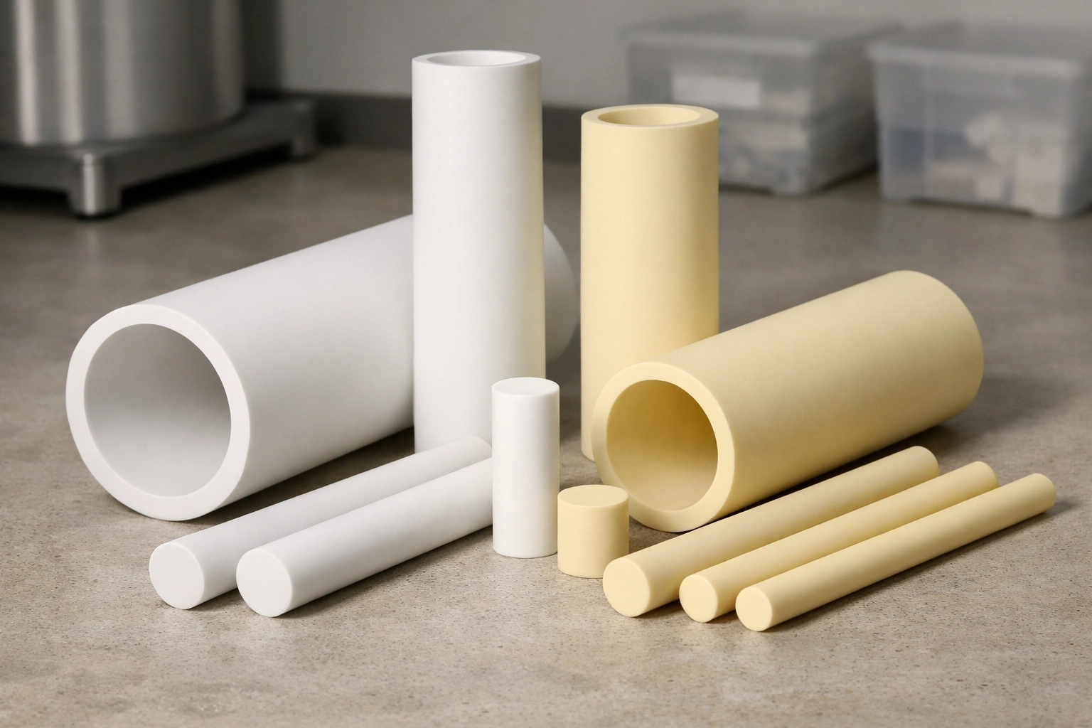
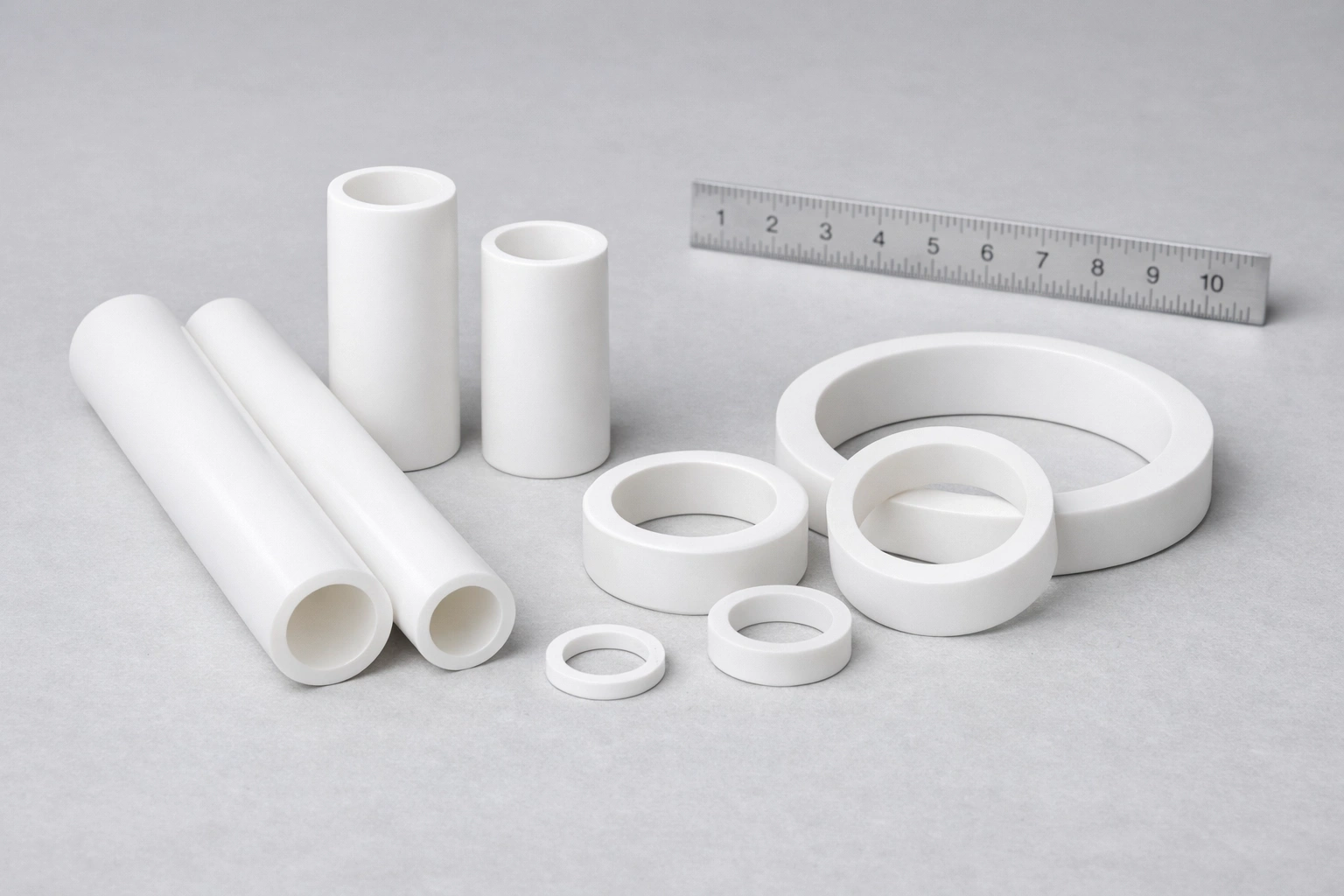
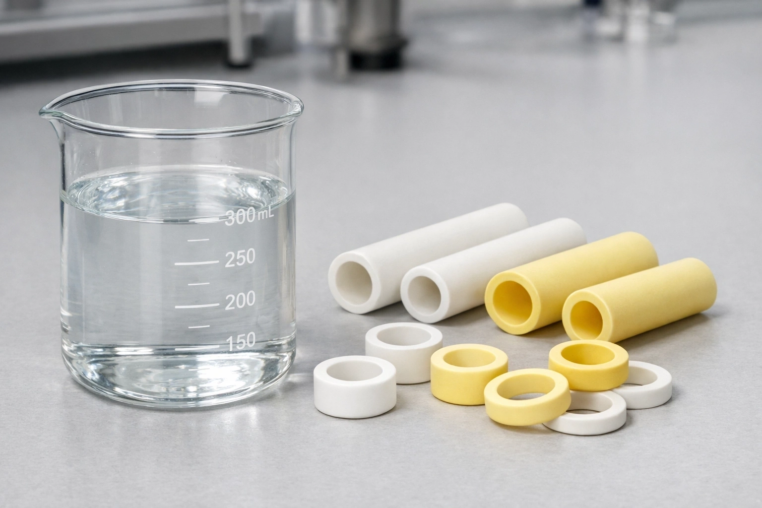
Broad thickness capability with small batch flexibility
ADCERAX supports Alumina Substrate thicknesses from 0.25 mm up to 1.20 mm, covering fast-response sensors, power electronics, and industrial insulation components. Small batch production enables customers to validate thickness selections through pilot runs before committing to volume manufacturing, reducing technical and commercial risk. -
Integrated process control across forming sintering and finishing
Thickness consistency is maintained through controlled forming, sintering, grinding, and inspection processes. By monitoring thickness deviation and flatness simultaneously, ADCERAX ensures that specified thickness delivers the intended electrical and mechanical behavior rather than only meeting dimensional criteria. -
Application aligned delivery and quality verification
Thickness solutions are delivered with inspection data aligned to application priorities, such as flatness for power modules or mechanical robustness for insulation parts. This approach allows engineers to verify thickness performance against real operating conditions instead of relying solely on nominal values.
In this way, ADCERAX positions thickness customization as an engineering solution that reduces uncertainty and accelerates qualification cycles.
Thickness Selection as Long Term Engineering Decision
Thickness selection for an Alumina Substrate influences system behavior long after initial qualification testing is complete. Consequently, thickness should be evaluated against lifetime loading, manufacturing variation, and service conditions rather than short-term performance metrics.
-
Thickness affects reliability progression over time
Substrates with marginal thickness margins often perform acceptably during early testing but develop cracks or warpage after extended thermal or mechanical cycling. Increasing thickness by 10–20% frequently delays such degradation mechanisms and stabilizes long-term behavior. -
Thickness decisions shape manufacturing resilience
Thickness that aligns with process capability reduces sensitivity to minor variation in sintering, grinding, or cutting. This resilience improves yield stability and lowers the likelihood of unexpected process drift during scale-up. -
Thickness reflects engineering priorities rather than cost alone
Although thicker substrates may increase material usage, they often reduce overall system risk. When evaluated over the full product lifecycle, optimized thickness selection supports predictable performance and lower total engineering effort.
Ultimately, thickness should be regarded as a long-term engineering commitment that underpins reliability, manufacturability, and system stability.
Conclusion
In essence, Alumina Substrate thickness defines the balance between electrical safety, thermal control, and mechanical reliability across diverse applications.
ADCERAX supports engineers with application-driven Alumina Substrate thickness customization, combining design insight, manufacturing control, and rapid delivery to meet real system requirements.
FAQ
What is the most common Alumina Substrate thickness used in industry?
Common thickness values range from 0.38 mm to 0.63 mm, offering balanced electrical, thermal, and mechanical performance for many applications.
Can Alumina Substrate thickness be adjusted without redesigning the entire system?
Yes. Incremental thickness changes of 0.05–0.20 mm often improve reliability without requiring major design modifications.
Does thicker Alumina Substrate always improve reliability?
Not always. Thickness must be matched to application priorities, since excessive thickness can increase thermal resistance without providing additional benefit.
When should custom thickness be considered instead of standard values?
Custom thickness is recommended when standard options lead to yield loss, warpage, or insufficient electrical or mechanical margins under real operating conditions.
References: