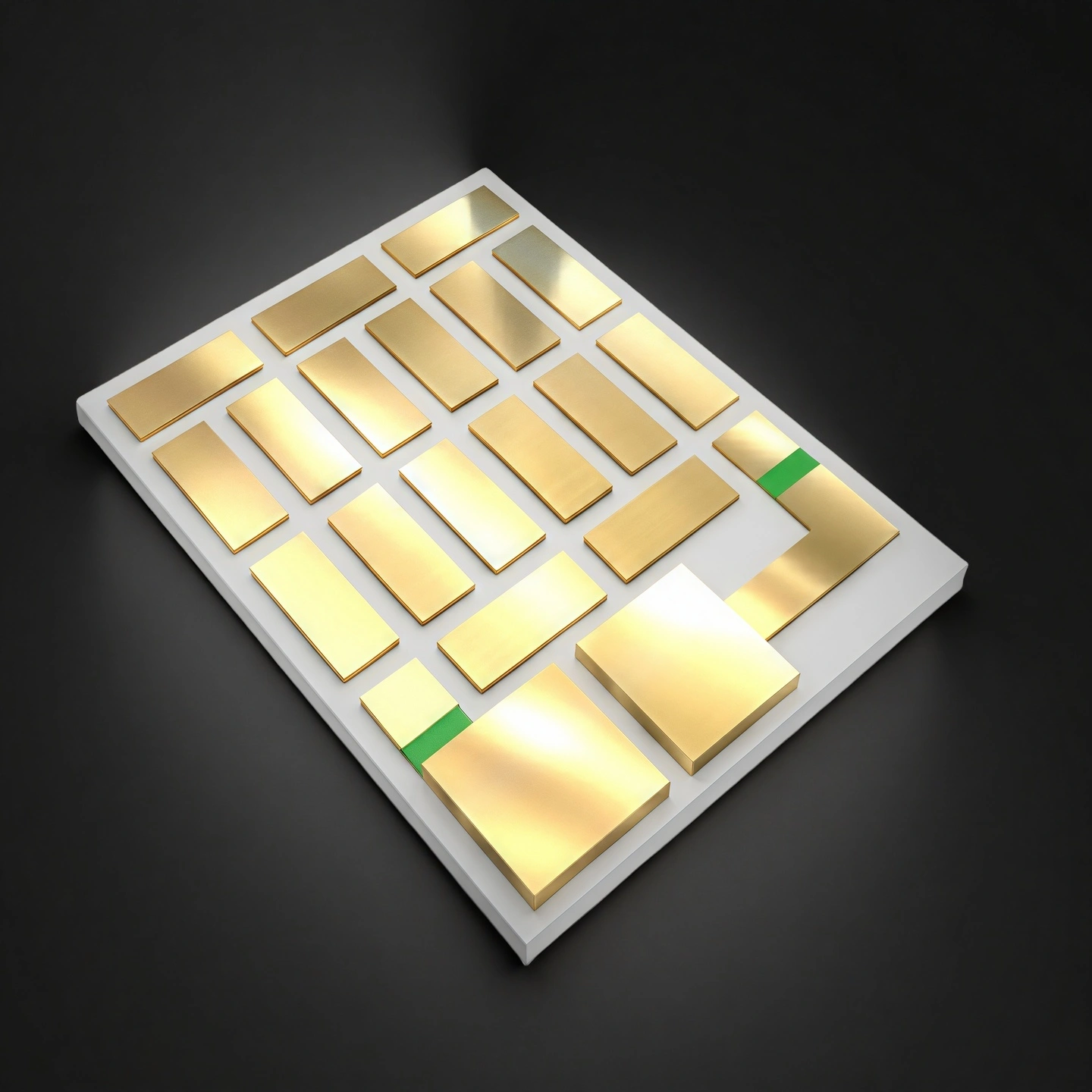
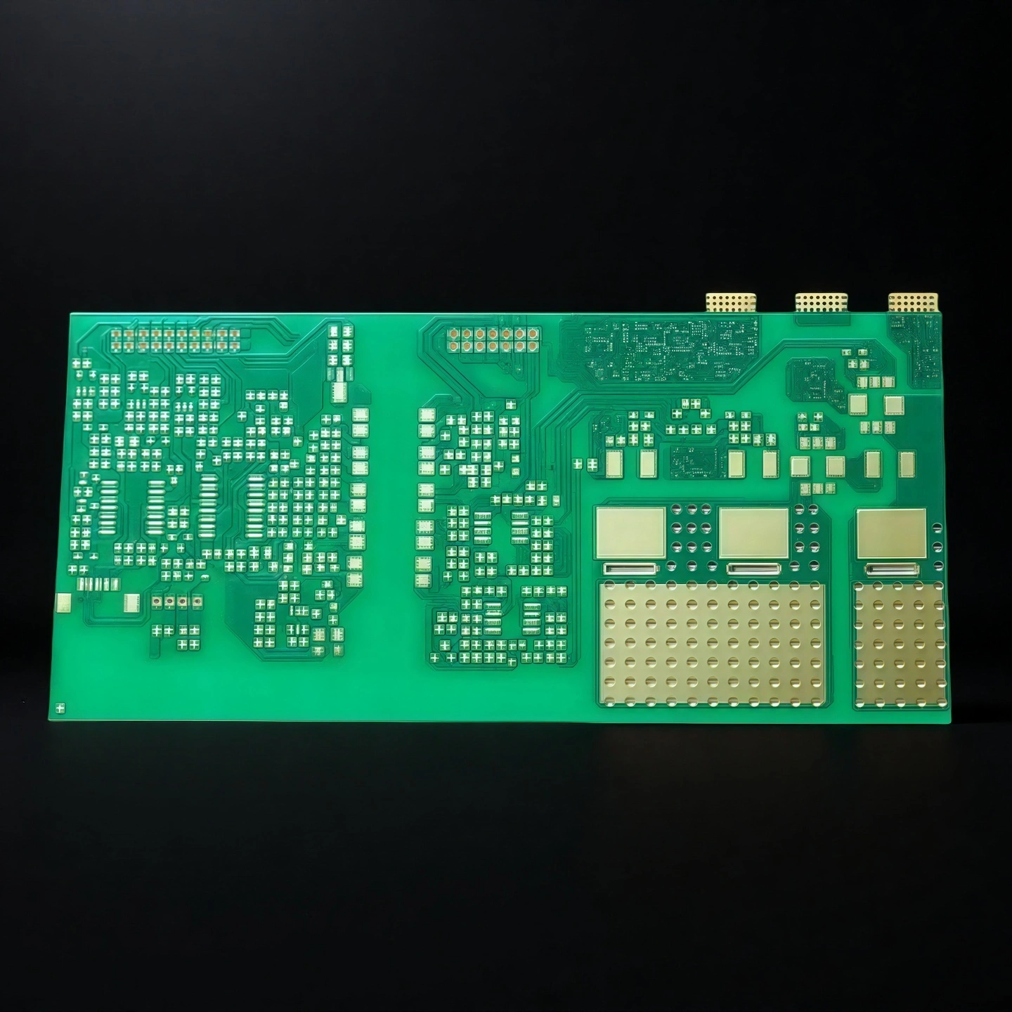
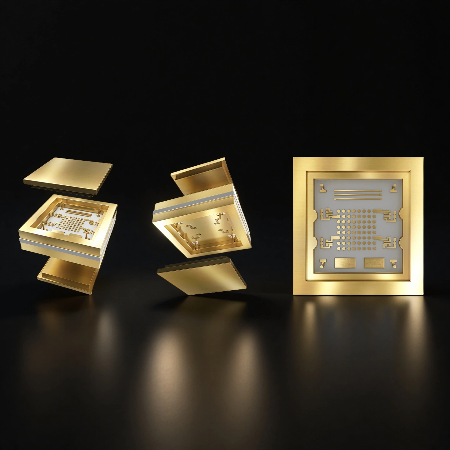
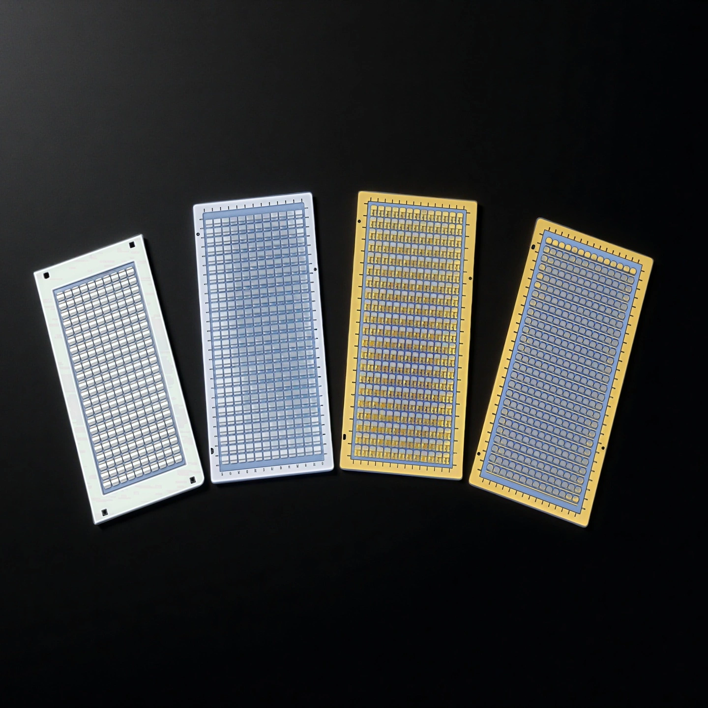
A metalized aluminum nitride substrate is a high thermal conductivity ceramic base with engineered metal patterns that provides electrical interconnection, insulation and heat spreading for power electronics, RF modules and high-power optoelectronic packages.
Metalized Aluminum Nitride Substrate Benefits
-
Efficient heat spreading
The metalized aluminum nitride substrate transfers heat away from power dies through a ceramic with thermal conductivity in the 170–200 W/m·K range, supporting compact layouts and lower junction temperatures. -
Matched CTE to power devices
The AlN base of the metalized substrate offers a coefficient of thermal expansion close to Si and SiC, which helps reduce thermo-mechanical stress during power cycling. -
Fine-line metallization on AlN
The metallized AlN substrate supports fine pad and trace geometries suitable for dense power modules, RF matching networks and LED arrays, with controllable line width and spacing. -
High dielectric strength under high voltage
The aluminum nitride ceramic body provides high dielectric strength and insulation resistance, allowing the metalized aluminum nitride substrate to carry high voltage while maintaining a compact footprint. -
Stable bond and solder interfaces
Optimized metallization stacks on the metalized AlN substrate support common joining methods such as soldering, wire bonding and sintered silver, maintaining adhesion under thermal cycling.
Metalized Aluminum Nitride Substrate Properties
| Property Content | Unit | Unit | ALN-170 | ALN-200 | ALN-230 |
| Basic Properties | Color | gray | light yellow | light yellow | |
| Density | g/cm³ | 3.2-3.3 | 3.2-3.3 | 3.2-3.3 | |
| Surface Roughness | μm | 0.2-0.75 | 0.2-0.75 | 0.2-0.8 | |
| Camber | length ‰ | ≤3‰ | ≤3‰ | ≤3‰ | |
| Hardness | HV | 1100 | 1100 | 1100 | |
| Thermal Properties | Max Operating Temperature | °C | 1100 | 1100 | 1100 |
| Thermal Conductivity | W/m·K | 170-190 | 190-220 | 220-230 | |
| Coefficient of Thermal Expansion | 10⁻⁶/K(20-400°c) | 4-5 | 4-5 | 4-5 | |
| Coefficient of Thermal Expansion | 10⁻⁶/K(400-800°c) | 5-6 | 5-6 | 5-6 | |
| Mechanical Properties | Flexural Strength | MPa | 300-400 | 350-450 | 400-500 |
| Tensile Strength | MPa | 200-300 | 250-350 | 280-380 | |
| Compressive Strength | MPa | 2000-3000 | 2200-3200 | 2500-3500 | |
| Electrical properties | Dielectric Constant | at 1MHz | 8-9 | 8-9 | 8-9 |
| Dielectric strength | KV/mm | ≥15 | ≥15 | ≥15 | |
| Volume resistivity | 20℃ Ω.cm | ≥1014 | ≥1014 | ≥1014 |
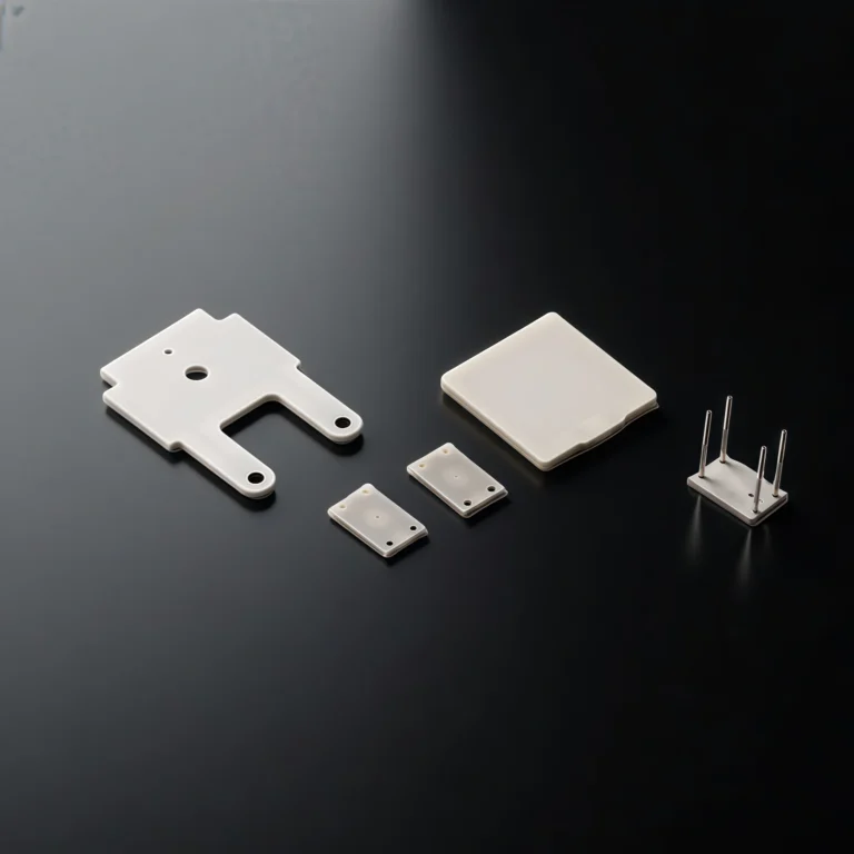
Metalized AlN Substrate Specifications
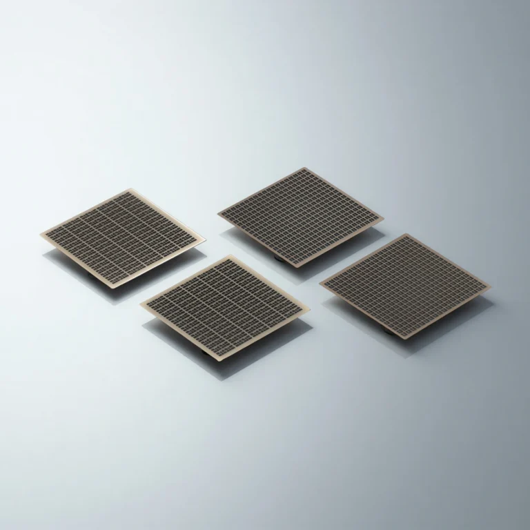
- Type 1—LED Packaging Substrate
| Name: | LED Packaging Substrate |
|---|---|
| Common Specifications: | 15-80 μm |
| Model: | AT-AlN-LJ1001 |
| Application Scenarios: | LED Packaging, Chip Packaging |
| Category | Item | Standard Specification | Special Specification |
|---|---|---|---|
| Substrate | Substrate Thickness | 0.38 ~ 1.0 mm | Min: 0.15 mm, Max: 2.0 mm |
| Machinable Outline Size Range | 114*114mm, 120*120mm | Min: 50.8*50.8 mm, Max: 138*190 mm | |
| Hole | Positioning Hole Control Deviation | ± 50 μm | Min: ± 20 μm |
| Via Diameter (Specific Ratio Dependent) | ≥ 100 μm | Min: 40 μm | |
| Hole Spacing | ≥ 300 μm (3 times hole diameter) | Min: 80 μm | |
| Via to Copper Edge | ≥ 70 μm | Min: 50 μm | |
| Circuit | Line Width | ≥ 80 μm | Min: 40 μm |
| Line Spacing | ≥ 80 μm | Min: 40 μm | |
| Tolerance Range | ± 25 μm | Min: ± 10 μm | |
| Outline | Outline Tolerance | ± 100 μm | Min: ± 50 μm |
- Type 2—Power Laser Diode (LD)
| Name: | Power Laser Diode (LD) |
|---|---|
| Common Specifications: | 15-80 μm |
| Model: | AT-AlN-GJ1001 |
| Application Scenarios: | Laser Lighting, Laser Projection/Display, Optical Communication, Unmanned Aerial Vehicles (UAV), 3D Gesture Recognition, 3D Sensing LiDAR |
- Type 3—Semiconductor Cooling Substrate TEC

| Name: | Semiconductor Cooling Substrate TEC |
|---|---|
| Common Specifications: | 1-20 μm |
| Model: | AT-AlN-TJ1001 |
| Application Scenarios: | Optical Communication/Temperature Control, Optoelectronic Device Heat Dissipation, Refrigerators, Thermoelectric Coolers, Thermoelectric Generation, etc. |
- Type 4—Automotive Radar Ceramic Substrate

| Name: | Automotive Radar Ceramic Substrate |
|---|---|
| Common Specifications: | Approximately 50 μm |
| Model: | AT-AlN-CJ1001 |
| Application Scenarios: | Automotive Sensors, Automotive Radar |
- Type 5—Ceramic Metal Tube Shell
| Name: | Ceramic Metal Tube Shell |
|---|---|
| Common Specifications: | 60-1000 μm |
| Model: | AT-AlN-K1001 |
| Application Scenarios: | Microcontrollers, Video Controllers, Crystal Filters, Logic Circuit Storage Devices, Integrated Amplifiers |
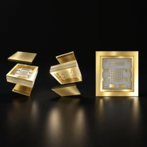
AlN Substrates Metallized Packaging
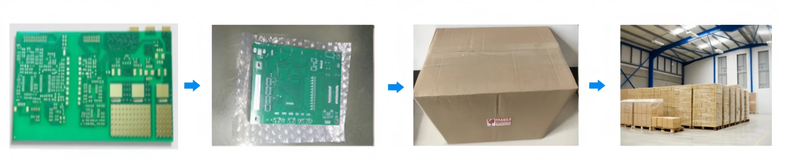
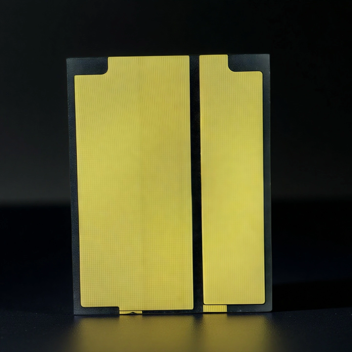
- Each metalized aluminum nitride substrate is separated in rigid plastic trays or cavity blister packs to prevent pad damage and edge chipping.