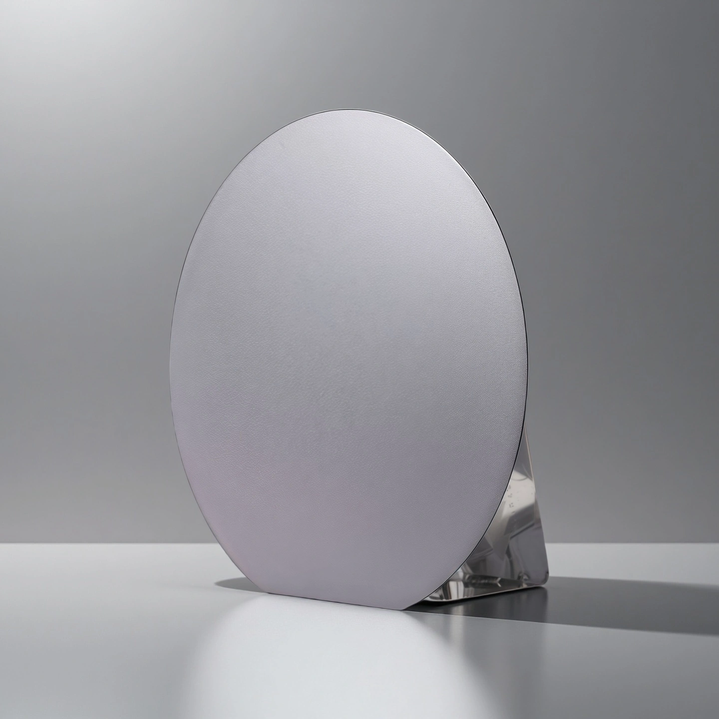
ADCERAX® Silicon Carbide Substrate supports advanced semiconductor development by combining wide-bandgap material characteristics with stable thermal, mechanical, and electrical behavior under demanding operating environments. Its crystal structure enables reliable performance in high-temperature, high-voltage, and high-frequency device architectures, allowing consistent functionality across power electronics, RF systems, and optoelectronic applications. These properties create a continuous performance path from material selection to device integration, ensuring predictable behavior throughout the full development cycle.
Advanced Material Characteristics of Silicon Carbide Substrate
- High Breakdown Field Capability
The material sustains electric fields above 3 MV/cm, allowing compact vertical device geometries.
- Wide Bandgap Operation
A bandgap of 3.2–3.4 eV maintains carrier stability under elevated junction temperatures.
- Stable Resistivity Control
Conductive and semi-insulating forms maintain resistivity within controlled engineering ranges, including values exceeding 10⁵ Ω·cm for RF isolation.
- High Elastic Modulus
The substrate maintains an elastic modulus between 450–470 GPa, ensuring limited deformation during processing.
- Low Thermal Expansion
The coefficient of thermal expansion remains within 4.0–4.6×10⁻⁶/K, limiting stress accumulation during rapid temperature transitions.
- Thermal Conductivity Advantage
Thermal conductivity between 120–160 W/m·K ensures efficient heat spreading under high power density.
- Low Micropipe Density
Advanced growth technologies reduce micropipe density to ppm-level, improving yield in vertical device fabrication.
- Controlled Surface Roughness
Epi-ready surfaces achieve polishing targets below 1 nm RMS, supporting uniform epitaxial layer formation.
- Flatness and Geometry Control
Wafer geometry parameters such as TTV, warp, and bow remain within tightly regulated engineering windows, often measured in micron-level ranges.
Technical Specifications of Silicon Carbide Substrate
The Silicon Carbide Substrate exhibits quantifiable physical, thermal, electrical, and structural characteristics that define its behavior in high-temperature, high-frequency, and high-power applications, allowing consistent performance analysis in laboratory and device-development environments.
| Property |
Specification |
| Crystal Structure |
Hexagonal (4H-SiC / 6H-SiC) |
| Bandgap |
3.2–3.4 eV |
| Breakdown Electric Field |
~3 MV/cm |
| Thermal Conductivity |
120–160 W/m·K |
| Coefficient of Thermal Expansion |
4.0–4.6 × 10⁻⁶ /K |
| Elastic Modulus |
450–470 GPa |
| Hardness |
Mohs ≈ 9 |
| Resistivity Range (Semi-Insulating) |
>10⁵ Ω·cm |
| Resistivity Range (Conductive) |
n-type / p-type engineered windows |
| Surface Roughness (Epi-Ready) |
<1 nm RMS |
| Micropipe Density |
ppm-level |
| Dielectric Constant |
~9.7 |
| Refractive Index |
2.6–2.7 |
| Thermal Shock Resistance |
High stability under rapid cycling |
| Chemical Resistance |
Stable in acid, alkali, and oxidizing media |
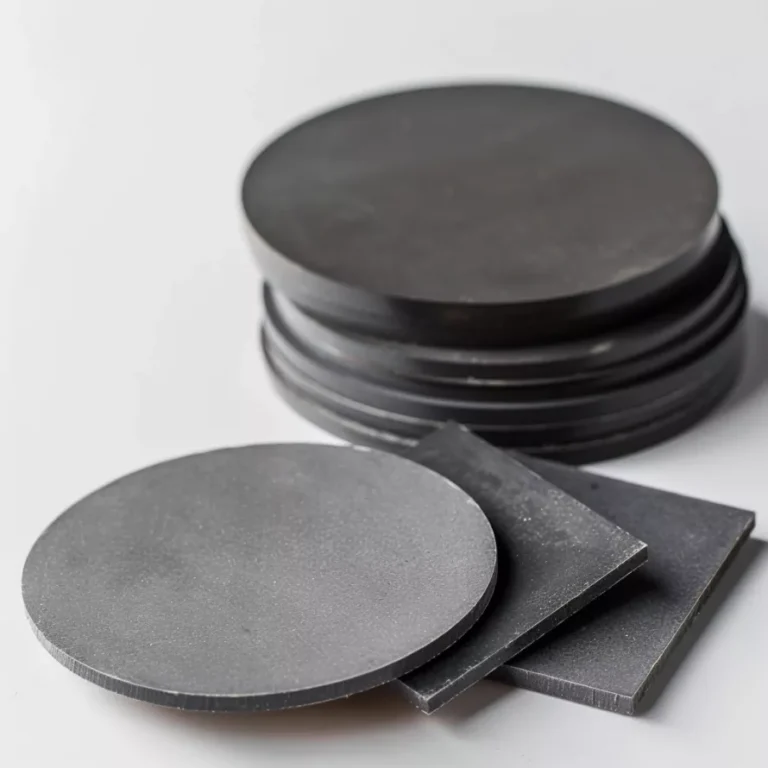
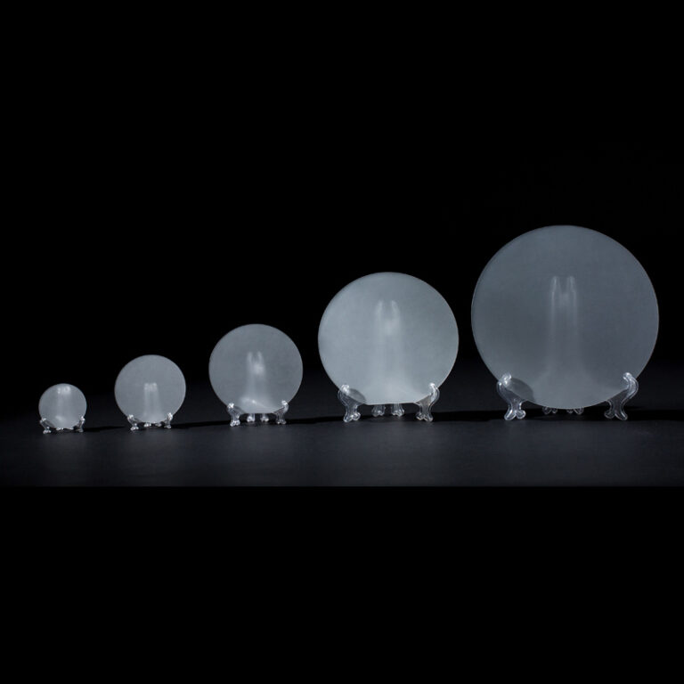
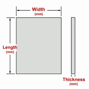
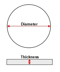
Dimensions of Silicon Carbide Substrate
| Sic Substrate Specifications |
| Growth Method |
Seed Crystal Sublimation Method, PVT (Physical Vapor Transport) |
| Crystal Structure |
Hexagonal |
| Lattice Constant |
a=3.08 Å c=15.08 Å |
| Stacking Sequence |
ABCACB |
| Orientation |
Growth Axis or Off-axis <0001> 3.5° |
| Band Gap |
2.93 eV (Indirect) |
| Hardness |
9.2 (Mohs) |
| Thermal Conductivity @300K |
5 W/cm·K |
| Dielectric Constant |
e(11)=e(22)=9.66 e(33)=10.33 |
| Dimensions |
10x3, 10x5, 10x10, 15x15, 20x15, 20x20, dia2", 15 x 15 mm, 10x10mm, etc. |
| Thickness |
0.5mm, 1.0mm |
| Polishing |
Single-sided or Double-sided |
| Crystal Orientation |
<001>±0.5° |
| Crystal Face Orientation Accuracy |
±0.5° |
| Edge Orientation Accuracy |
2° (Special requirements can reach within 1°) |
| Off-cut Wafer |
Wafers with edge-oriented crystal faces can be processed at a specific angle (tilt angle 1° - 45°) according to specific requirements. |
| Ra: |
≤5Å (5μm×5μm) |
| Packaging |
Class 100 clean bag, Class 1000 cleanroom |
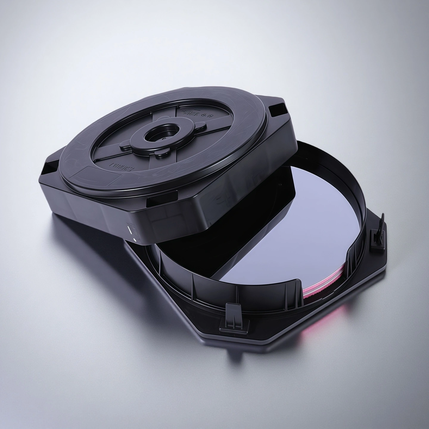
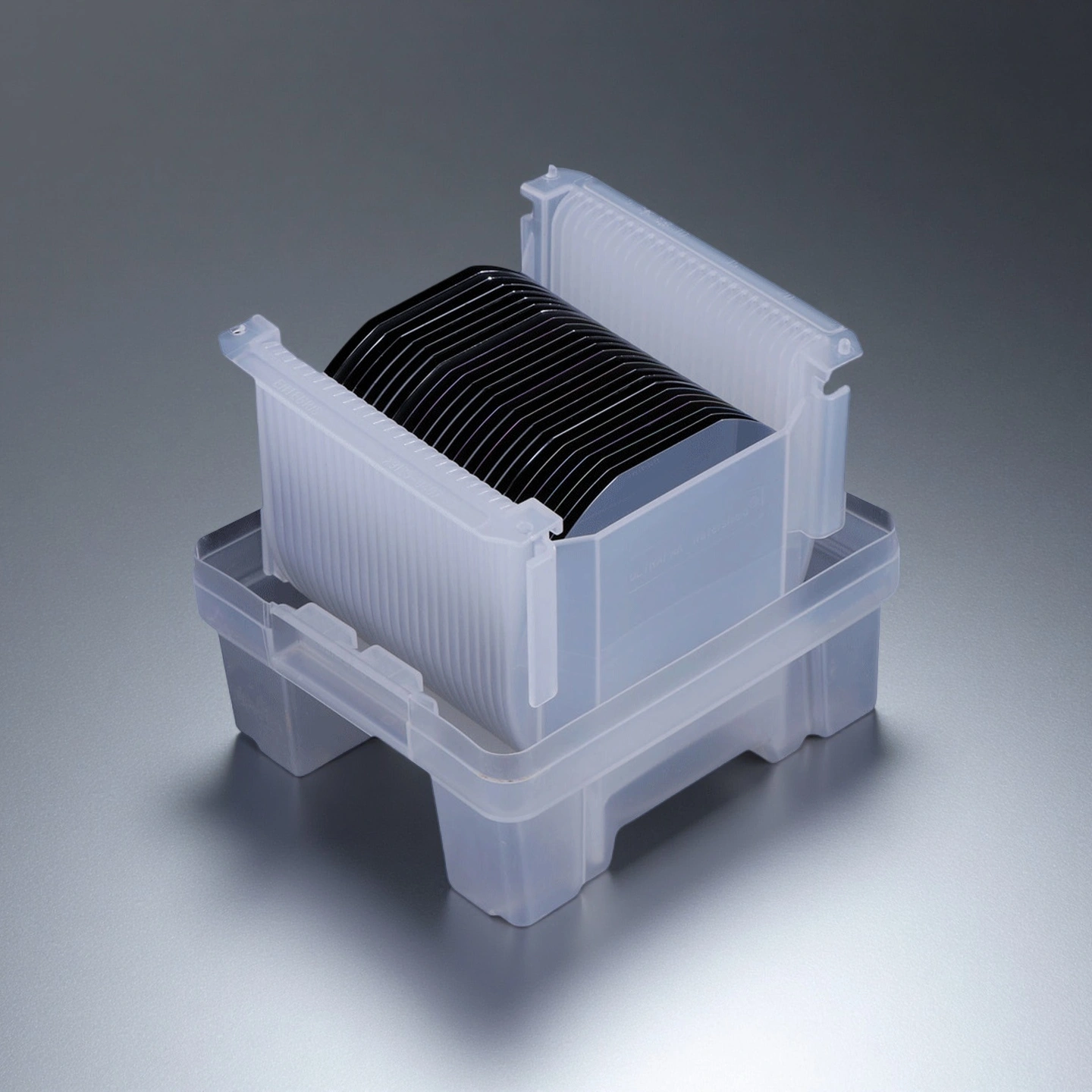
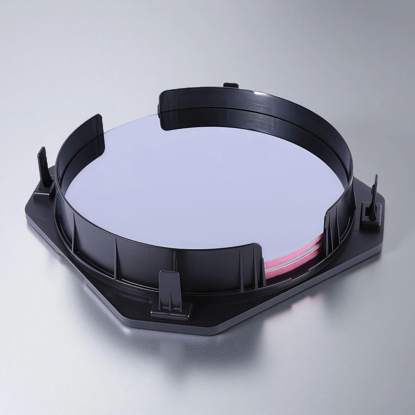
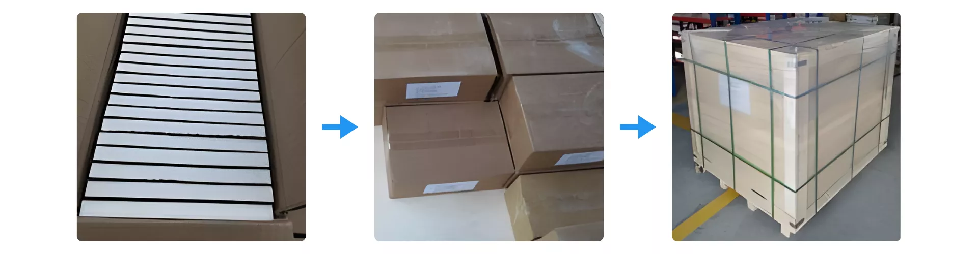
Protective Packaging for Silicon Carbide Substrate
Silicon Carbide Substrate is packed through a multi-stage protective system to ensure stability during long-distance transportation. Each substrate is first placed in individual reinforced cartons, which are then consolidated into labeled shipping boxes to maintain traceability. All boxed units are finally secured on palletized frames with full perimeter strapping to prevent vibration, compression, or impact throughout the global logistics process.
ADCERAX® Silicon Carbide Substrate Overcomes Critical Performance Challenges in Real Industrial Devices
The Silicon Carbide Substrate supplied by ADCERAX® enables stable operation in high-stress electrical, thermal, and environmental conditions, allowing engineering teams to resolve measurable bottlenecks in power conversion, RF output stability, and high-temperature sensing reliability across demanding industrial systems.
-
Silicon Carbide Substrate in EV Traction Inverters and High-Power Converters
✅Key Advantages
1. Wide-Temperature Junction Stability
The wide bandgap of 3.2–3.4 eV allows devices on ADCERAX® Silicon Carbide Substrate to maintain stable switching behavior at elevated junction temperatures. In traction inverter simulations, device characteristics remained within tight limits when junction temperature profiles were extended beyond 175 °C under repeated acceleration cycles.
2. High-Field Compact Device Layout
A breakdown electric field close to 3 MV/cm supports higher blocking voltages without increasing chip area. This electrical margin enables designers to shrink die size while maintaining target voltage ratings, which helps reduce conduction path length and supports higher power density platforms.
3. Efficient Heat Spreading Under Cycling
Thermal conductivity in the range of 120–160 W/m·K improves heat spreading from hotspots generated during rapid current transients. In high-power converter layouts, this property helped reduce peak temperature rise at critical nodes by more than 10–15 °C, supporting more stable operation during frequent start–stop and regenerative braking events.
✅ ️Problem Solved
An EV inverter development team reported recurring thermal runaway risk when using conventional substrates, with junction temperature spikes exceeding safe limits during repeated high-current ramps. Under endurance testing, modules showed accelerated degradation after several hundred thermal cycles, and switching losses increased as heat concentration intensified in localized areas. After migrating the power stage to ADCERAX® Silicon Carbide Substrate, thermal mapping showed peak junction temperatures reduced by approximately 10–15 °C at comparable load conditions. Long-cycle tests indicated a significant reduction in parameter drift, and projected module lifetime under automotive drive cycles improved by more than 50 % based on accelerated stress data.
-
Silicon Carbide Substrate in 5G RF Power Amplifiers and Microwave Systems
✅Key Advantages
1. High-Resistivity Semi-Insulating Base
Semi-insulating ADCERAX® Silicon Carbide Substrate can reach resistivity values above 10⁵ Ω·cm, providing a stable isolation platform for GaN-on-SiC RF structures. This high-resistivity base helps suppress substrate conduction paths that would otherwise cause gain compression and reduced isolation in dense RF front ends.
2. Low RF Loss with Stable Dielectric Behavior
A dielectric constant around 9.7 combined with a low-loss tangent, often targeted below 0.01 at microwave frequencies, supports cleaner RF transmission. In amplifier layouts, this behavior contributes to more consistent gain and lower insertion loss across multi-carrier 5G bands compared with lower-performance substrate options.
3. Thermal Management for Dense RF Arrays
Thermal conductivity between 120–160 W/m·K enhances heat removal from high-power RF transistors concentrated in compact amplifier modules. This property helps keep channel temperature rise under control when average RF output power is increased, supporting higher output levels without exceeding device thermal design limits.
✅ ️Problem Solved
A communication equipment manufacturer observed that base station RF power amplifiers built on conventional substrates exhibited noticeable gain droop and phase drift after extended full-load operation. Thermal imaging showed localized hotspots in the transistor region, and long-duration tests recorded output power variation approaching 1 dB over a continuous operating period. After switching the PA module design to ADCERAX® semi-insulating Silicon Carbide Substrate, RF measurements over the same stress profile indicated gain variation reduced to below 0.2 dB. At the same time, case and junction temperatures in the active region dropped by approximately 8–10 °C, and overall amplifier efficiency increased by several percentage points at the target output power level.
-
Silicon Carbide Substrate in High-Temperature Industrial Sensors and Control Modules
✅Key Advantages
1. Stable Structure at Elevated Temperature
With a coefficient of thermal expansion of 4.0–4.6×10⁻⁶/K, ADCERAX® Silicon Carbide Substrate maintains dimensional stability under repeated exposure to high furnace and reactor temperatures. This controlled expansion behavior limits stress on bonded sensor elements when operating in environments that routinely exceed 600 °C.
2. High Modulus Against Mechanical Drift
An elastic modulus in the range of 450–470 GPa provides strong resistance to bending and warpage under thermal and mechanical load. In sensor assemblies, this stiffness helps keep alignment and strain transfer paths consistent over thousands of thermal cycles, reducing zero-shift and span drift in measurement output.
3. Chemical Inertness in Corrosive Media
The material remains stable in acidic and alkaline atmospheres across a typical pH window from 2 to 12, and exhibits high resistance to oxidizing gases at elevated temperature. Prolonged exposure tests above 500 °C in aggressive flue gas compositions show minimal surface degradation, supporting long-term sensor encapsulation integrity.
✅ ️Problem Solved
A process control integrator deploying high-temperature gas sensors in industrial furnaces reported that previous substrate solutions suffered from structural distortion and surface attack after extended exposure, leading to calibration drift and frequent sensor replacement. Over several months of operation, measurement offset increased significantly after repeated thermal cycling, and maintenance teams were forced to recalibrate or swap sensors at short intervals. After redesigning the sensing element on ADCERAX® Silicon Carbide Substrate, endurance testing over more than 1 000 thermal cycles demonstrated a marked reduction in drift, with full-scale deviation remaining below 0.1 % in controlled trials. Field feedback showed that calibration intervals could be extended by a factor of 2–3, reducing downtime and improving continuity of process monitoring in harsh industrial environments.
ADCERAX® Silicon Carbide Substrate User Guide for Safe and Optimal Operation
The Silicon Carbide Substrate requires controlled handling, environmental awareness, and process-aligned preparation to ensure stable performance throughout device fabrication and integration. This guidance helps users navigate critical steps that influence substrate integrity, thermal behavior, electrical stability, and long-term operational reliability.
-
Handling and Pre-Process Preparation Guidelines
1. Controlled Surface Contact
Avoid direct contact with the active surface to prevent contamination that may disrupt epitaxial uniformity. Use cleanroom gloves and certified handling tools to maintain a controlled interface. Implement a dedicated substrate tray to prevent micro-abrasion before processing.
2. Cleanroom Environment Requirements
Follow ISO-class cleanroom protocols to limit particle adhesion that may impact downstream processing. Ensure air filtration and humidity control remain within acceptable stability thresholds. Store unused substrates in sealed carriers to maintain environmental integrity.
3. Inspection Before Production
Perform a visual and optical inspection to confirm no visible microcracks or edge chips. Use non-contact metrology tools to verify flatness consistency prior to high-temperature procedures. Document incoming conditions to support traceability throughout manufacturing.
-
hermal Management and Temperature Transition Practices
1. Gradual Temperature Ramping
Apply controlled heating and cooling profiles to avoid thermal shock that could induce internal stress. Use programmable furnace curves aligned with substrate thermal expansion behavior. Monitor temperature uniformity across the load to maintain repeatable thermal conditions.
2. High-Temperature Exposure Control
Keep peak operating temperatures within system-defined safe boundaries to maintain crystal stability. Ensure thermal gradients across the substrate remain minimal during power cycles. Validate furnace or reactor calibration to prevent localized overheating.
3. Post-Thermal Inspection Requirements
After exposure to high-temperature processes, confirm no warpage or distortion using precision metrology systems. Review any surface changes that may affect downstream device layers. Record all thermal cycle parameters to support quality documentation.
-
Chemical Compatibility and Cleaning Recommendations
1. Approved Cleaning Agents
Use non-corrosive solvents or solutions tested for chemical compatibility with Silicon Carbide. Avoid aggressive etchants unless specifically required for a controlled process step. Rinse thoroughly with deionized water to prevent residue accumulation.
2. Safe Handling of Reactive Environments
When substrates encounter acidic, alkaline, or oxidizing atmospheres, verify chamber stability and leak integrity. Monitor exposure times to avoid unnecessary chemical stress. Utilize protective storage containers to minimize environmental impact between steps.
3. Contamination Prevention Measures
Prevent metal, organic, or particulate contamination that could compromise electrical isolation and epitaxial adhesion. Establish dedicated workflows for substrate transfer and cleaning. Conduct periodic audits of workstation cleanliness to ensure repeatability.
-
Storage, Transport, and Long-Term Preservation
1. Secure Packaging Protocols
Store substrates in shock-absorbing carriers designed to protect edges and polished surfaces. Use properly sealed containers to guard against airborne particles. Maintain vertical stacking limits to avoid mechanical pressure accumulation.
2. Environmental Storage Conditions
Preserve substrates in temperature-stable, low-humidity environments to avoid moisture-related surface anomalies. Monitor storage room cleanliness and airflow systems to maintain consistency. Implement periodic environmental validation checks to ensure compliance.
3. Transport Safety and Traceability
Use certified logistics packaging that minimizes vibration and compression during shipment. Ensure each batch includes traceable labeling for quality reference across global transit. Conduct post-arrival inspection to verify substrate condition before use.