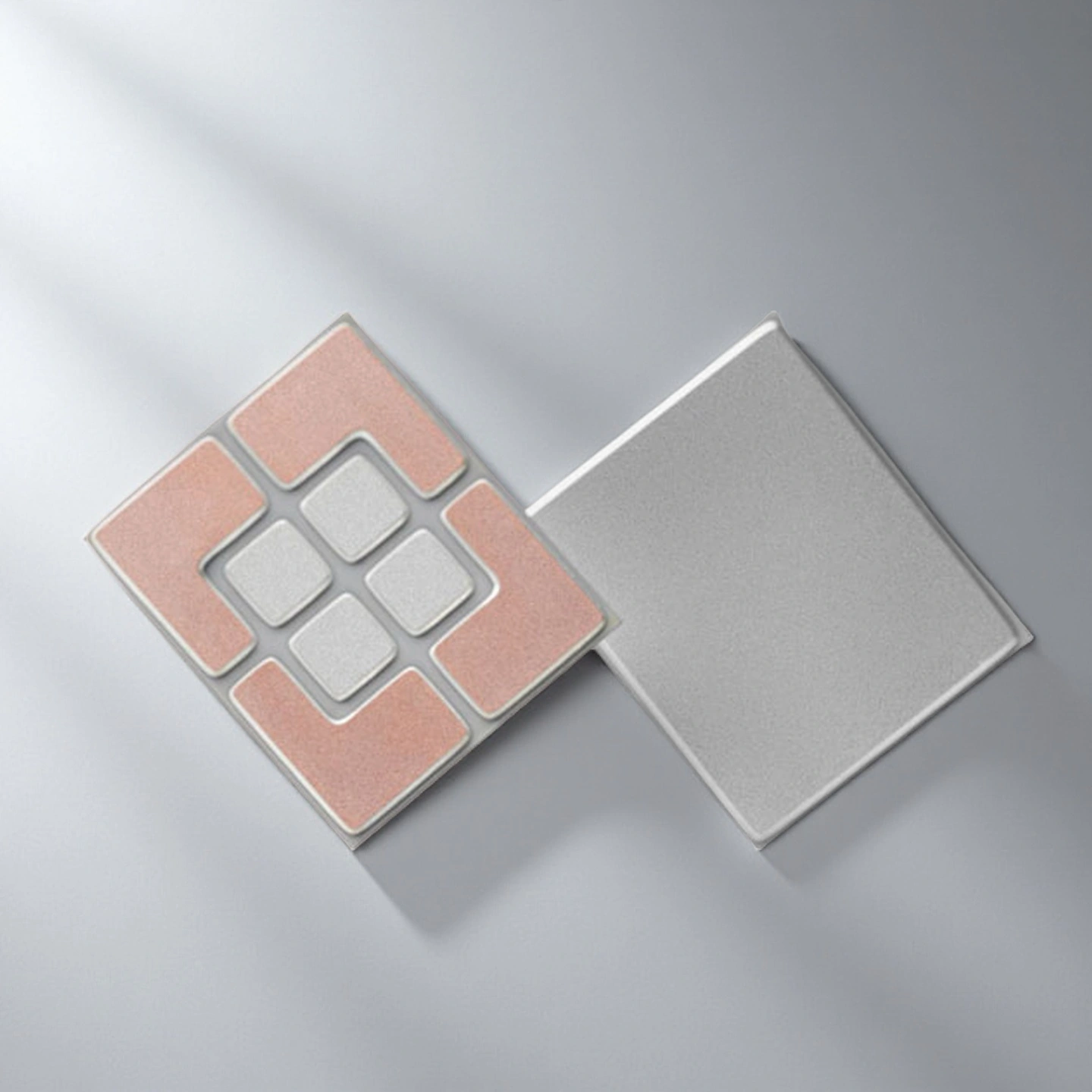
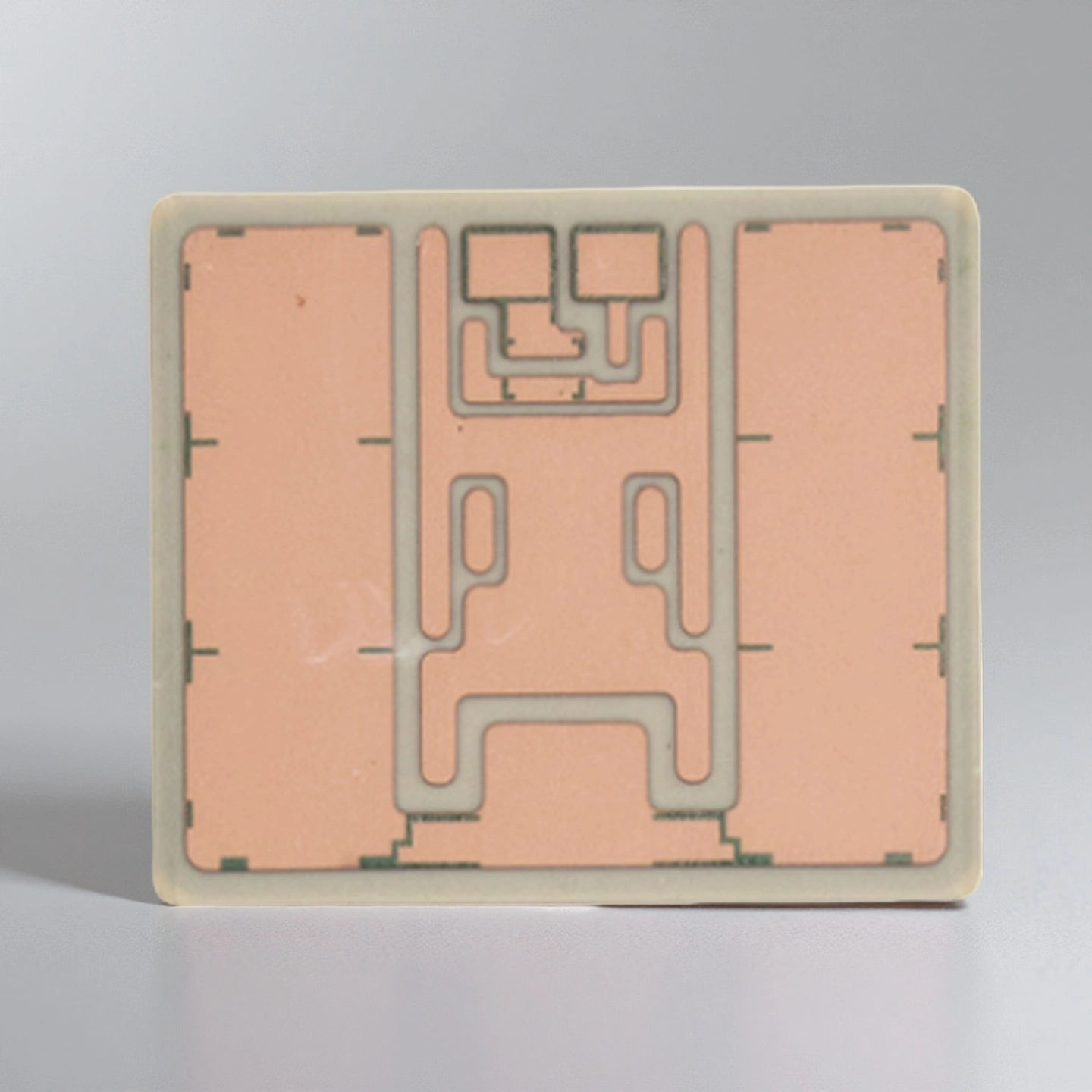
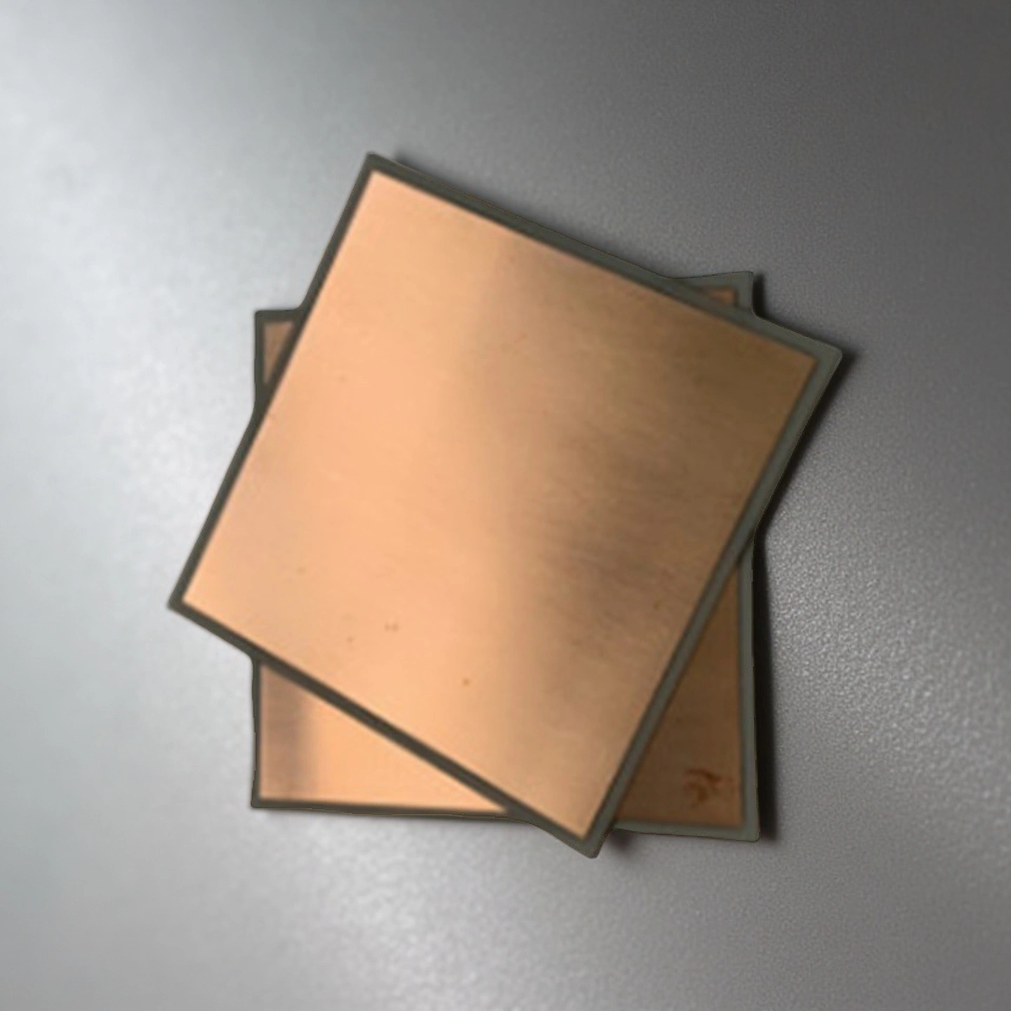
AMB silicon nitride substrate combines high thermal conductivity, low thermal expansion, and high bending strength, making it suitable for high-power semiconductor modules that undergo repeated thermal cycling. Compared with Al₂O₃ or AlN DBC substrates, silicon nitride AMB boards provide higher fracture toughness and longer power cycling life. It is widely used in traction inverters, on-board chargers, DC/DC converters, wind power converters, and industrial servo drives.
AMB Silicon Nitride Substrate Benefits
-
High Power Cycling Reliability
The silicon nitride AMB substrate maintains mechanical and electrical stability beyond 10,000 thermal cycles from -40 °C to 150 °C under SiC and IGBT power module operation. The high fracture toughness of Si₃N₄ prevents dielectric layer cracking, while oxygen-free copper maintains contact resistance below 0.1 mΩ during repeated current loading. -
Low Warpage After Copper Brazing
Panel-level warpage typically remains within 20–30 µm after active metal brazing and cooling, even with 300 µm or 500 µm copper thickness. This flatness level supports pressure-assisted silver sintering and ensures uniform solder thickness in vacuum reflow processes. -
CTE Matching with SiC Semiconductor Chips
The thermal expansion coefficient of 2.7–3.2×10⁻⁶/K closely aligns with SiC MOSFET chips (≈4.0×10⁻⁶/K), minimizing thermal stress between chip and substrate during rapid temperature rises and high-current switching cycles. This reduces chip–substrate delamination and extends module lifetime. -
High Mechanical Strength and Crack Resistance
Silicon nitride exhibits a flexural strength above 800 MPa and fracture toughness of 6–8 MPa·m¹ᐟ². This resists edge chipping, ultrasonic cleaning damage, and mechanical stress during module mounting or screw fastening—an advantage over brittler Al₂O₃ and AlN ceramics. -
Supports Thick Copper for High Current Designs
The AMB process allows 70 µm to 500 µm of copper on one or both sides. Thick copper supports current levels above 400–800 A, reduces thermal resistance from junction to baseplate, and enables planar busbar integration in SiC traction inverters or energy storage converters.
AMB Si₃N₄ Substrate Properties
| Si3N4 Type | Gas pressure sintering Si3N4 | Hot pressing sintering Si3N4 | High thermal conductivity Si3N4 |
| Density (g/cm3) | 3.2 | 3.3 | 3.25 |
| Flexture strength (MPa) | 700 | 900 | 600~800 |
| Young Modulus (GPa) | 300 | 300 | 300~320 |
| Poisson's ratio | 0.25 | 0.28 | 0.25 |
| Compressive strength (MPa) | 2500 | 3000 | 2500 |
| Hardness (GPa) | 15 | 16 | 15 |
| Fracture toughness (MPa*m1/2) | 5~7 | 6~8 | 6~7 |
| Maximum working temperature (℃) | 1100 | 1300 | 1100 |
| Thermal conductivity (W/m*K) | 20 | 25 | 80~100 |
| Thermal expansion coefficient (/℃) | 3*10-6 | 3.1*10-6 | 3*10-6 |
| Thermal shock resistance (ΔT ℃) | 550 | 800 | / |
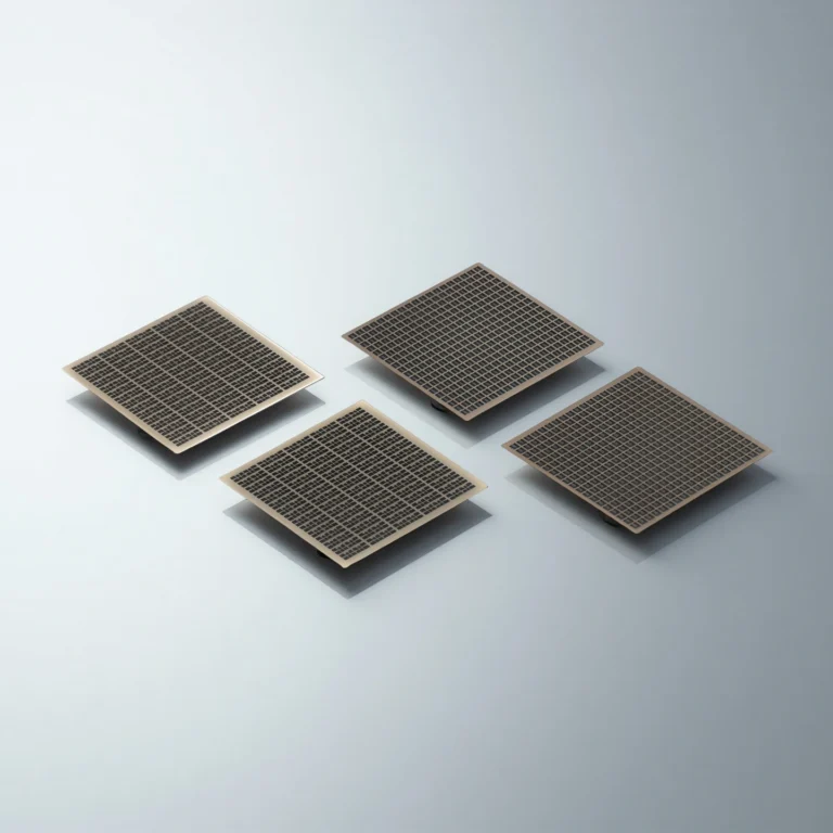
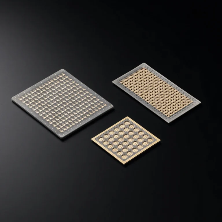
Silicon Nitride AMB Substrate Specifications
Part 1: Processing Accuracy for Silicon Nitride Substrate AMB Copper Clad
| Item | Specification | |
|---|---|---|
| Copper layer surface roughness | Ra≤1.5μm, Rz≤10μm, Rmax=50μm | |
| Coating layer | Nickel | 2-10μm (P6%-10%) |
| Silver | 0.1-1.0μm | |
| Nickel-gold | Ni: 2-10μm, Au: 0.01-0.15μm | |
| Nickel-gold-palladium | Ni: 2-10μm, Au: 0.01-0.15μm, Pd: 0.01-0.15μm | |
| Solder mask | Line width, space, tolerance | ≥0.2mm, tolerance ±0.2mm |
| Position tolerance | ±0.2mm | |
| Thickness | 5-40μm | |
| Temperature change endurance | ≤320℃/10s | |
Part 2: AMB Silicon Nitride Substrate Size
| AMB Silicon Nitride Substrate | |||
| Item No. | Length*Width(mm) | Thickness(mm) | Copper layer thickness(mm) |
| AT-SIN-FT1001 | 10*10——127*178 | 0.25 | 0.127、0.2、0.25、0.3、0.4、0.5、0.8 |
| AT-SIN-FT1002 | 0.32 | ||
| AT-SIN-FT1003 | 0.38 | ||
| AT-SIN-FT1004 | 0.63 | ||
| AT-SIN-FT1005 | 1.0 | ||
| AT-SIN-FT1006 | Other thickness customization | ||
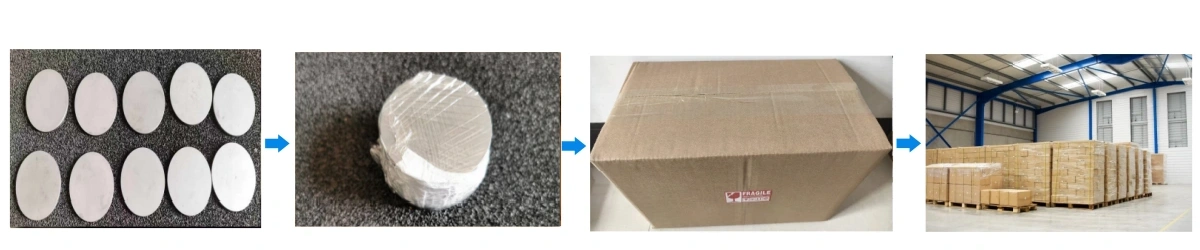
AMB Si₃N₄ Substrate Packaging
- Each Si3N4 active metal brazed substrate is sealed in anti-static packaging.
- Packed in foam-lined boxes to prevent mechanical damage.