Custom Beryllium Oxide Substrates with Via/Slot/Chamfer Features | High-Thermal-Conductivity BeO

High-thermal-conductivity beryllium oxide substrates for RF power, microwave modules, SiC/GaN power electronics, and photonics packaging, supplied as standard squares (10×10, 25×25, 50×50 mm; 0.25–1.0 mm) or fully customized with metal patterns, vias, and surface finishes. Typical thickness windows 0.25–1.0 mm with ±0.02–0.05 mm thickness control and flatness control on request; metallization patterns and edge features produced per drawing to fit RF and power-module footprints.

Catalogue No. AT-BeO-J1001
Material Beryllium Oxide
Thermal Conductivity ≥220 W/mK
Maximum Operating Temperature 1000°C+
Dimensions/Sizes Download PDF
24H Standard Dispatch
Small Batch Support OEM
Factory Direct
Expert Engineering Support

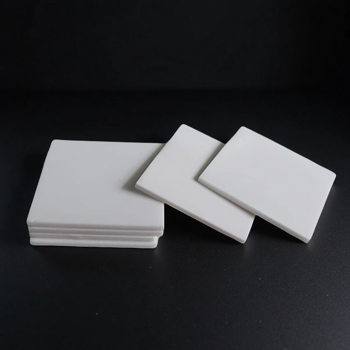
Beryllium Oxide (BeO) substrates are ceramic baseplates used as the electrical-insulating, heat-spreading foundation in high-power and high-frequency assemblies (RF/microwave power amplifiers, SiC/GaN power modules, laser/photonics packages, thick-film hybrid circuits).

Advantages of Beryllium Oxide Substrates

  • High heat flux capability — ceramic k≈200–280 W/m·K enables compact die attach with reduced thermal resistance.
  • Stable RF dielectric — εr≈6.5–7.2, low loss for repeatable line widths and pad capacitance.
  • Controlled planarity — flatness and surface roughness tuned for uniform TIM/braze bond-lines.
  • Metallization compatibility — Au/Ag/Ni/Au patterning suitable for thick-film, soldering, and active brazing.
  • Feature integration — vias, slots, countersinks, and chamfers reduce secondary machining at the module level.


Beo Ceramic Substrate Properties

Property Be-97 Be-99
BeO Purity ≧97% ≧99%
Density (g/cm3) ≧2.85 ≧2.85
Hardness (Hv) 1200 1250
Maximum Working Temperature (℃) 1600 1650
Flexural Strength (MPa) 170 190
Fracture Toughness (MPa*m1/2) 2.5~3.5 2.5~3.5
Dielectric Constant (at 1MHz) 6.5 7
Breakdown Voltage (kV/mm) 15 20
Thermal Conductivity (W/m*K) 220-240 260-310
Thermal Expansion Coefficient (/℃) 7~8.5*10-6 7~8.5*10-6


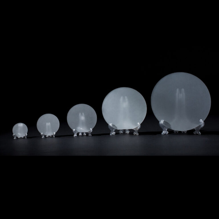
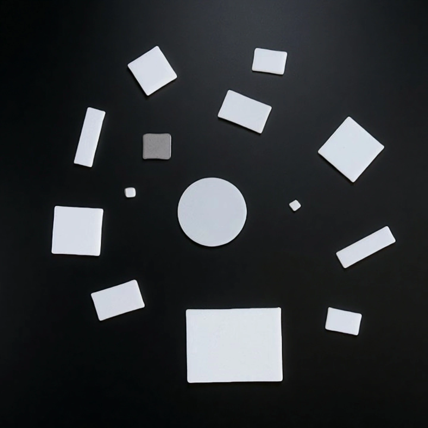
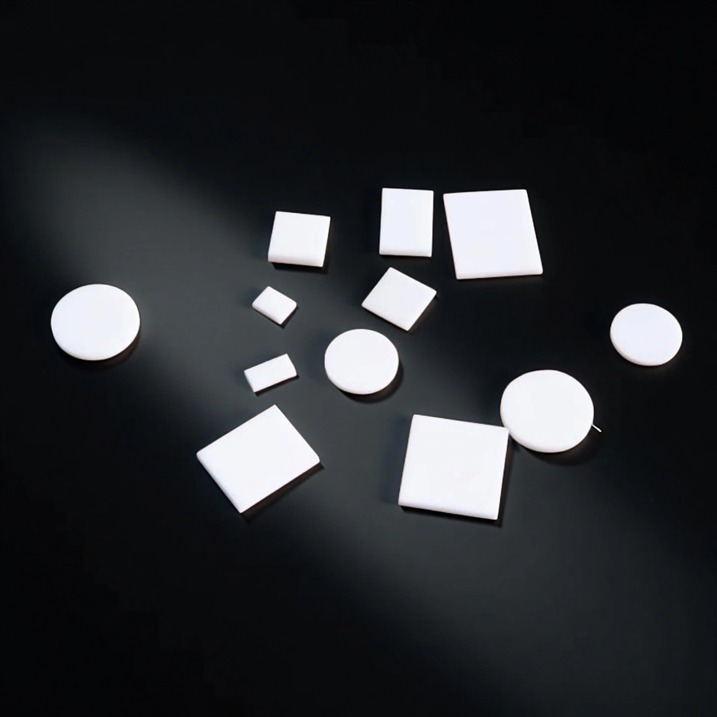
Specifications of Beo Substrates

Type 1-Square Beo Substrates 
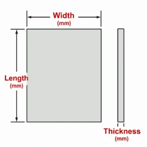
size for substrate

Item Length*Width(mm) Thickness(mm)
AT-BeO-J1001 50.8*50.8 0.38
AT-BeO-J1002 76.2*76.2 0.38
AT-BeO-J1003 101.6*101.6 0.38
AT-BeO-J1004 114.3*114.3 0.38
AT-BeO-J1005 32.1*9 0.5
AT-BeO-J1006 40*9 0.5
AT-BeO-J1007 45*2.5 0.5
AT-BeO-J1008 50.8*50.8 0.5
AT-BeO-J1009 76.2*76.2 0.5
AT-BeO-J1010 101.6*101.6 0.5
AT-BeO-J1011 114.3*114.3 0.5
AT-BeO-J1012 7*6 0.635
AT-BeO-J1013 40*30 0.635
AT-BeO-J1014 42*42 0.635
AT-BeO-J1015 50.8*50.8 0.635
AT-BeO-J1016 76.2*76.2 0.635
AT-BeO-J1017 101.6*101.6 0.635
AT-BeO-J1018 114.3*114.3 0.635
AT-BeO-J1019 25.5*19.5 1
AT-BeO-J1020 27*18.2 1
AT-BeO-J1021 36.7*9.7 1
AT-BeO-J1022 46.8*22.4 1
AT-BeO-J1023 50.8*50.8 1
AT-BeO-J1024 76.2*76.2 1
AT-BeO-J1025 101.6*101.6 1
AT-BeO-J1026 114.3*114.3 1
AT-BeO-J1027 12.7*10 1.5
AT-BeO-J1028 30*30 1.5
AT-BeO-J1029 50.8*50.8 1.5
AT-BeO-J1030 76.2*76.2 1.5
AT-BeO-J1031 101.6*101.6 1.5
AT-BeO-J1032 114.3*114.3 1.5


Type 2-Round Beo Substrates 
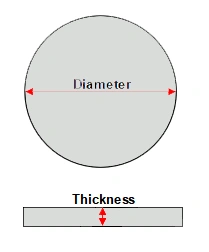
size for substrate

Item Diameter(mm) Thickness(mm)
AT-BeO-J2001 20 1.0 
AT-BeO-J2002 26 1.0 
AT-BeO-J2003 30 1.0 
AT-BeO-J2004 35 1.0 
AT-BeO-J2005 50 1.0 
AT-BeO-J2006 52 1.0 
AT-BeO-J2007 60 1.0 
AT-BeO-J2008 75 1.0 
AT-BeO-J2009 100 1.0 
AT-BeO-J2010 110 1.0 
AT-BeO-J2011 20 1.2 
AT-BeO-J2012 26 1.2 
AT-BeO-J2013 30 1.2 
AT-BeO-J2014 35 1.2 
AT-BeO-J2015 50 1.2 
AT-BeO-J2016 52 1.2 
AT-BeO-J2017 60 1.2 
AT-BeO-J2018 75 1.2 
AT-BeO-J2019 100 1.2 
AT-BeO-J2020 110 1.2 
AT-BeO-J2021 20 1.5 
AT-BeO-J2022 26 1.5 
AT-BeO-J2023 30 1.5 
AT-BeO-J2024 35 1.5 
AT-BeO-J2025 50 1.5 
AT-BeO-J2026 52 1.5 
AT-BeO-J2027 60 1.5 
AT-BeO-J2028 75 1.5 
AT-BeO-J2029 100 1.5 
AT-BeO-J2030 110 1.5 
AT-BeO-J2031 20 2.0 
AT-BeO-J2032 26 2.0 
AT-BeO-J2033 30 2.0 
AT-BeO-J2034 35 2.0 
AT-BeO-J2035 50 2.0 
AT-BeO-J2036 52 2.0 
AT-BeO-J2037 60 2.0 
AT-BeO-J2038 75 2.0 
AT-BeO-J2039 100 2.0 
AT-BeO-J2040 110 2.0 
AT-BeO-J2041 20 2.5 
AT-BeO-J2042 26 2.5 
AT-BeO-J2043 30 2.5 
AT-BeO-J2044 35 2.5 
AT-BeO-J2045 50 2.5 
AT-BeO-J2046 52 2.5 
AT-BeO-J2047 60 2.5 
AT-BeO-J2048 75 2.5 
AT-BeO-J2049 100 2.5 
AT-BeO-J2050 110 2.5 
AT-BeO-J2051 20 3.0 
AT-BeO-J2052 26 3.0 
AT-BeO-J2053 30 3.0 
AT-BeO-J2054 35 3.0 
AT-BeO-J2055 50 3.0 
AT-BeO-J2056 52 3.0 
AT-BeO-J2057 60 3.0 
AT-BeO-J2058 75 3.0 
AT-BeO-J2059 100 3.0 
AT-BeO-J2060 110 3.0 


Beryllium Oxide Substrates Packing

  • Clean-room bag + shock-absorbing tray; hazard labeling per BeO HSE handling guidance.

Beryllium Oxide Substrates Packing


Applications of Beryllium Oxide Substrates

  • RF / Microwave / Radar Modules

    ✅Key Advantages

    1. Thermal path under die: k≈200–280 W/m·K shortens junction-to-case path at high power.
    2. Dielectric stability: εr≈6.5–7.2 supports controlled impedance layouts.
    3. Assembly yield: flatness control reduces voids in braze/TIM.

    ✅ Problem Solved

    An RF PA module scaling from 80 W to 160 W increased heat flux above 100 W/cm². Switching to 0.5 mm BeO with tighter flatness cut junction temperature by ≈10–15 °C at equal airflow, reducing rework by >30% over three pilot lots and lifting output power margin without enlarging the housing.

  • SiC/GaN Power Electronics

    ✅Key Advantages

    1. High heat-flux cycling: supports >200 W/m·K heat spreading in compact baseplates.
    2. CTE compatibility: ≈7.5–8.0 ppm/K mitigates stress against die/leadframe.
    3. Metallization options: Ni/Au pads aligned with active braze and solder attach.

    ✅ Problem Solved

    A 30 kW inverter’s baseplate hotspot limited current at ΔTcase≈18 °C. A 50×50×1.0 mm BeO baseplate dropped Rθ by ≈15–20%, enabling the same output at ≈3–4 °C lower case temperature and stabilizing thermal cycling results across >100 assemblies.

  • Laser/Photonics Packaging

    ✅Key Advantages

    1. Localized heat spreading: protects emitter junctions during CW operation.
    2. Surface quality control: lapped finishes support thin bond-line repeatability.
    3. Low loss path: reduces parasitic heating in high-frequency drivers.

    ✅ Problem Solved

    A pump-laser seat suffered bond-line variability causing ±6 °C junction drift. Switching to lapped BeO and fixed pad metallization cut spread to ±2 °C, improving optical output stability and reducing post-burn-in rejects by ≈40%.

Usage Instructions for Beo Ceramic Substrate

  • Install

    1. Before assembly, inspect each substrate for surface chips or contamination; verify thickness, flatness, and metallization against the QC report.
    2. Always handle substrates by edges using tweezers or vacuum pens; avoid touching active surfaces or pads to prevent oil contamination.
    3. For die attach or brazing, use compatible Au, Ag, or Ni/Au metallized surfaces; ensure preforms and fluxes are residue-free.
    4. Maintain bond-line thickness ≤50–100 µm using calibrated spacers or controlled-pressure fixtures to ensure uniform heat transfer.
    5. During assembly, limit fixture pressure to <2 MPa to prevent micro-cracks. Confirm flatness contact with optical interferometer or feeler-gauge inspection before firing.
    6. For hybrid circuits, align printing masks precisely — even ±0.05 mm pad offset can affect impedance matching in RF designs.

  • Use

    1. Confirm the thermal stack-up: BeO substrate → solder/braze → die → lid or housing. The heat path should remain continuous without voids.
    2. Continuously monitor case temperature (Tc) during load tests. For RF and SiC modules, maintain ΔTj-Tc ≤25 °C for optimal reliability.
    3. Avoid sharp mechanical stress or localized heating; BeO ceramics have high strength but low fracture strain — twisting or point loading can induce cracks.
    4. When integrating into power modules or laser packages, ensure CTE matching (BeO ~7.5 ppm/K) with copper, molybdenum, or Kovar interfaces.
    5. Never drill, grind, or cut BeO in open environments. Machining must be done under sealed extraction systems compliant with HSE regulations.

  • Store

    1. Store in dry, temperature-controlled rooms (20–25 °C; RH < 60%) to prevent moisture absorption or metallization oxidation.
    2. Keep substrates in original anti-static, vacuum-sealed bags with desiccant; reseal after partial use.
    3. Avoid stacking heavy boxes; compression above 3 kg per tray may cause edge chipping or bowing.
    4. Retain traceability labels and inspection certificates with the same batch to simplify later validation or warranty claims.

  • Clean

    1. Use only non-abrasive solvent wipes (IPA or acetone) and lint-free cloths; never use alkaline cleaners or ultrasonic baths on metallized parts.
    2. If particle contamination occurs, blow off with filtered, oil-free nitrogen at ≤1 bar.
    3. For oxide surfaces (non-metalized), deionized-water rinse and warm-air drying at ≤100 °C can be applied.
    4. Avoid re-polishing or re-lapping after metallization — it alters pad thickness and adhesion strength.

  • Cautions

    1. BeO ceramic is classified as hazardous when powdered or abraded; intact sintered parts are safe to handle. Do not saw, sand, or break the substrates.
    2. Follow BeO HSE handling guidance for disposal: collect scrap separately in sealed bags labeled “Beryllium-Containing Waste.”
    3. Always wear nitrile gloves and safety glasses when unpacking or handling large plates.
    4. Dispose of desiccant and packaging according to local environmental protocols — avoid mixing with general waste.
    5. Ensure operators are trained in hazard communication (HazCom) and material-specific safety data sheet (MSDS) awareness.

Beryllium Oxide Substrates FAQ

  1. Q: What makes beryllium oxide substrates different from alumina or AlN ceramics?
    A: BeO substrates provide thermal conductivity up to 200–280 W/m·K, about 5× higher than alumina (Al₂O₃) and 20–40% higher than AlN, while keeping a similar dielectric constant (εr≈6.5–7.2). This combination enables higher power density in RF, laser, and SiC/GaN modules without sacrificing insulation or footprint size.
  2. Q: What dielectric performance can I expect in RF or microwave circuits?
    A: At 1 MHz–10 GHz, BeO maintains εr≈6.7 ±0.2 and tan δ < 0.0003, ensuring low loss and stable impedance for high-frequency hybrid circuits, power amplifiers, and radar transmit/receive modules.
  3. Q: What metallization systems are available and how are they selected?
    A: Typical options include Au, Ag, and Ni/Au.
    a. Au: corrosion-resistant and brazing-compatible.
    b. Ag: economical for thick-film circuits.
    c. Ni/Au: balanced adhesion + solderability for power modules.
    Selection depends on brazing alloy, operating temperature, and bonding process.

  4. Q: Can BeO substrates be machined after sintering?
    A: Only under controlled, enclosed extraction systems due to BeO dust toxicity. ADCERAX delivers fully machined and finished parts, eliminating the need for customer-side cutting or drilling.
  5. Q: How should BeO substrates be handled safely in production lines?
    A: Finished substrates are inert and safe when intact. Always handle with gloves or vacuum tweezers, avoid impact or abrasion, and do not break or grind them. Disposal and machining follow BeO HSE handling guidance with labeled waste segregation.

Beryllium Oxide Substrates Reviews

  • ⭐️⭐️⭐️⭐️⭐️
    We transitioned two microwave PA designs to beryllium oxide substrates. Flatness control improved bond-line uniformity, and thermal headroom increased without changing the housing.
    Emily Hart — Packaging Engineer, Northridge RF Systems
  • ⭐️⭐️⭐️⭐️⭐️
    ADCERAX supplied metallized BeO baseplates per our drawing. Unit variation stayed within tolerance, which simplified qualification across three inverter frames.
    Marco Díaz — Purchasing Manager, Vectra Drives
  • ⭐️⭐️⭐️⭐️⭐️
    For laser diode seats, the lapped BeO substrates heat spreader kept junction temperatures stable during long CW runs. The measured spread matched our model.
    Sofia Tan — R&D Lead, PhotonCore Labs
  • ⭐️⭐️⭐️⭐️⭐️
    Repeat lots of BeO substrates arrived with consistent thickness and pad geometry. The inspection packet helped close our PPAP faster.
    David Klein — Operations Director, Helion Power Modules
customize size

Beryllium Oxide Substrates Customized

Each BeO substrate can be tailored for specific thermal, RF, and assembly requirements. Dimensional accuracy, metallization design, and surface control ensure consistent performance across high-reliability power and microwave applications. What You Can Specify:

1. Planform & Thickness

  • Geometry: squares, rectangles, discs, or custom outlines.
  • Thickness range: 0.25–1.0 mm (others on request).
  • Tolerance: ±0.02–0.05 mm, verified per-lot with CMM inspection.
  • Edge configuration: chamfered, radiused, or straight-cut to prevent chip propagation.

2. Flatness / Warpage

  • Controlled to ≤0.05–0.10 mm across diagonal depending on substrate area.
  • Measured under optical interferometer or granite reference plate.
  • Optimized for vacuum clamping, die-bonding, and brazing consistency.

3. Surface Finish

  • Options: as-fired, ground, lapped, or polished.
  • Typical roughness: Ra 0.1–0.8 µm, customized for metallization or adhesive interfaces.
  • Edge deburring or micro-chamfering available to minimize particulate generation.

4. Metallization

  • Available stacks: Au, Ag, Ni/Au, or Cu-Mo bonding layers.
  • Compatible with solder, epoxy, and active brazing.
  • Patterning tolerance: ±0.05 mm for fine-feature designs.
  • Optional adhesion testing, solderability check, and pad thickness certification.

5. Through/Via & Features

  • Via holes, slots, pockets, countersinks, fiducials, serial markings, or alignment notches.
  • Hole diameters down to 0.2 mm, positional accuracy within ±0.03 mm.
  • Suitable for hermetic feedthroughs and multi-layer interconnects.

6. Tolerance Schema

  • Defined per drawing for hole size, position, pad-to-edge spacing, Ra limits, and coplanarity.
  • Optional GD&T (Geometric Dimensioning & Tolerancing) support for high-precision assembly.
  • Lot-specific inspection reports available on request.

Related Products

ADCERAX - Your Trusted Advanced Ceramics Manufacturing Partner

Direct factory manufacturing with comprehensive ceramic materials expertise and global supply capabilities

Direct Factory Manufacturing

China-based ceramic materials production facility with state-of-the-art equipment

Engineering Team

Experienced professionals in advanced ceramics applications and custom design

Quality Control

Strict quality control standards for technical ceramics manufacturing and quality management

Global Supply Chain

Serving customers worldwide with technical ceramics and rapid response

24/7 Technical Support

Round-the-clock support for ceramic components inquiries and technical assistance

500+ Satisfied Customers

Trusted by global customers for advanced ceramic materials and precision components

Get in touch with us

Our team will be happy to respond to you in less than 24 hours.

Adcerax's factory

Quick Quotation

*Our team will answer your inquiries within 24 hours.

*Your information will be kept strictly confidential.

Ready to Solve Your Engineering Challenge?

Partner with ADCERAX for reliable, high-performance advanced ceramic solutions. Our engineers are ready to discuss your project.

E-mail

info@adcerax.com

Phone

+(86) 0731-74427743 | WhatsApp: +(86) 19311583352

Response Time

Within 24 hours

Quick Quote

The more details you provide, the faster we can quote.

*We respond within 24 hours. All inquiries are confidential.

Download Catalog

Get Your Custom Sulution

The more details you provide, the faster we can respond.

customize size

*We respond within 24 hours. All inquiries are confidential.

Download Catalog