Custom Optical Communication Module AlN Substrate with Fine Metallization

The optical communication module AlN substrate is a high thermal conductivity aluminum nitride ceramic submount for TOSA/ROSA, QSFP/OSFP and silicon photonics optical modules, supplied in standard size ranges with fully customized dimensions, cavity features and metallization layouts according to customer drawings.

Catalogue No. AT-GT001
Material  Aluminum Nitride
Thermal Conductivity ≥170 W/m·K
Coefficient of Thermal Expansion (CTE) 4.5–5.5 × 10⁻⁶ /K (20–300 °C)
Flexural Strength ≥ 300 MPa
24H Standard Dispatch
Small Batch Support OEM
Factory Direct
Expert Engineering Support

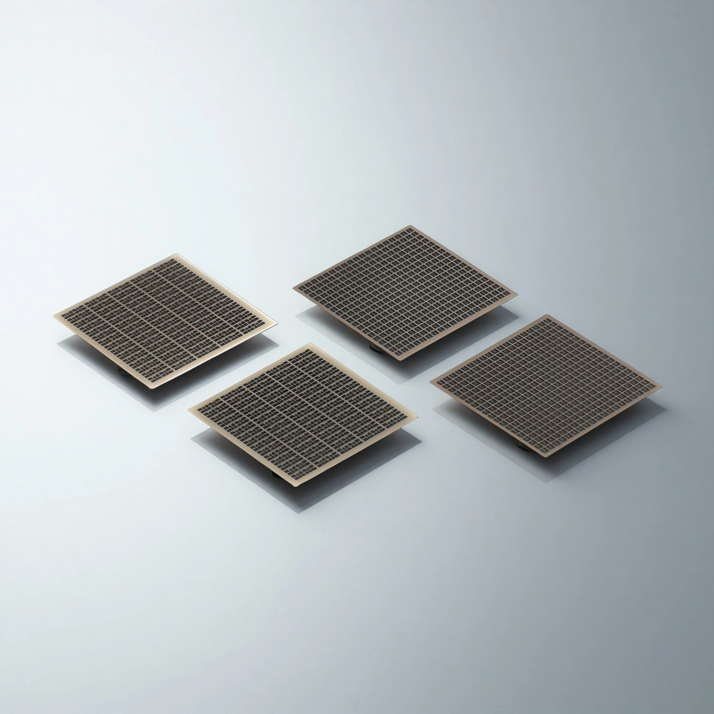
An optical communication module AlN substrate is a high-thermal-conductivity aluminum nitride ceramic submount or base plate used inside optical transceivers and optical communication modules (such as SFP, QSFP, OSFP, TOSA/ROSA, BOSA, AOC/ACC, and silicon photonics engines).

Optical Communication Module AlN Substrate Benefits

  • Thermal path matched to high-speed optics
    The optical communication module AlN substrate maintains high thermal conductivity in a thin profile, helping keep laser diode and SiPh junction temperatures several degrees lower than standard alumina-based submounts at comparable power levels.

  • CTE compatibility with optical chips
    The AlN substrate offers a thermal expansion behavior close to silicon and GaAs, which supports long-term reliability for die attach and reduces the risk of solder fatigue or die cracking under temperature cycling.

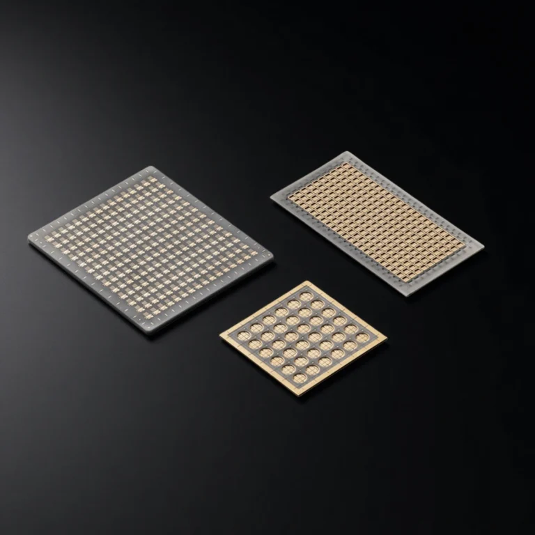
  • High flatness and tight dimensional tolerances
    Optical communication module AlN substrates can be manufactured with controlled flatness and typical dimensional tolerances in the ±0.02–0.05 mm range, supporting automated pick-and-place and active alignment processes inside optical modules.

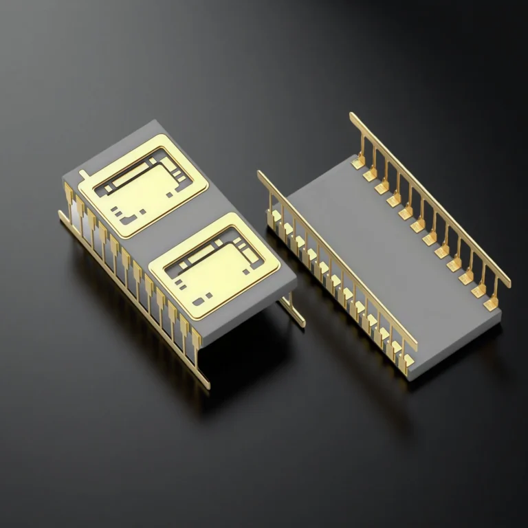
  • Fine metallization patterns for dense layouts
    The product supports fine-line metallization and via structures for compact optical communication module layouts, including differential signal routing and ground shielding around TOSA/ROSA or SiPh regions.

  • Thin and robust for compact pluggable formats
    The combination of high flexural strength and thin thickness capability allows the optical communication module AlN substrate to fit into constrained QSFP, OSFP and small-form-factor designs without compromising mechanical stability.


Optical Communication Module AlN Substrate Properties

Property Content Unit Unit ALN-170 ALN-200 ALN-230
Basic Properties Color gray light yellow light yellow
Density g/cm³ 3.2-3.3 3.2-3.3 3.2-3.3
Surface Roughness μm 0.2-0.75 0.2-0.75 0.2-0.8
Camber length ‰ ≤3‰ ≤3‰ ≤3‰
Hardness HV 1100 1100 1100
Thermal Properties Max Operating Temperature °C 1100 1100 1100
Thermal Conductivity W/m·K 170-190 190-220 220-230
Coefficient of Thermal Expansion 10⁻⁶/K(20-400°c) 4-5 4-5 4-5
Coefficient of Thermal Expansion 10⁻⁶/K(400-800°c) 5-6 5-6 5-6
Mechanical Properties Flexural Strength MPa 300-400 350-450 400-500
Tensile Strength MPa 200-300 250-350 280-380
Compressive Strength MPa 2000-3000 2200-3200 2500-3500
Electrical properties Dielectric Constant at 1MHz 8-9 8-9 8-9
Dielectric strength KV/mm ≥15 ≥15 ≥15
Volume resistivity 20℃ Ω.cm ≥1014 ≥1014 ≥1014


Optical Communication Module AlN Substrate Specifications

Aluminum Nitride Substrate
Item no. Substrate Dimension Thickness Machinable Aperture Fine Line Resolution Surface Roughness Metal Hole Protrusion Height Direction Identifier
AT-GT001 50.8*50.8±0.15 0.2-3.0mm Φ0.008mm ≥100μm ≤0.05μm ≤3μm with


Optical Communication Module Aluminum Nitride Substrate Packaging

  • Each optical communication module AlN substrate is separated in multi-cavity plastic trays or blister packs to avoid edge chipping and pad surface contact.

Optical Communication Module Aluminum Nitride Substrate Packaging

Optical Communication Module AlN Substrate Applications

  • Data Centre and AI Server Optical Transceivers

    ✅Key Advantages

    1. Junction Temperature Control in 400G/800G Modules
    The optical communication module AlN substrate can reduce laser diode junction temperature by several degrees compared with alumina submounts at the same output power, supporting higher lane speeds and power budgets.
    2. Support for High Port Density Pluggables
    AlN substrates allow thin, compact submount designs so that dense front-panel QSFP and OSFP modules can maintain thermal performance without oversized heat sinks.
    3. Stable Performance under Continuous Operation
    With appropriate thermal design, modules using the optical communication module AlN substrate can run continuously at high traffic load with controlled temperature drift over long service periods.

    ✅ Problem Solved

    A data centre operator deploying hundreds of 400G and 800G ports can experience several watts of heat per module. When alumina-based submounts are used, internal junction temperatures may run 5–10 °C higher at full load, reducing laser lifetime and increasing field failure rates. By redesigning the optical engine around an optical communication module AlN substrate, the module vendor can lower junction temperatures, keep module case temperatures within the thermal budget and maintain the required bit error rate at high ambient conditions. This supports higher rack density and reduces replacement events over a typical three-to-five-year deployment cycle.

  • Telecom Backbone and Metro Optical Communication Equipment

    ✅Key Advantages

    1. CTE-Matched Substrate for Long-Term Stability
    The optical communication module AlN substrate provides a CTE close to silicon and GaAs, which helps maintain stable die attach in systems that experience repeated daily and seasonal temperature swings.
    2. Suitability for Long-Reach and Coherent Modules
    For long-haul or coherent optical communication modules, the thermal behaviour of the AlN substrate contributes to stable optical performance and phase control.
    3. Improved Reliability Under Field Conditions
    Modules using AlN submounts can maintain low failure rates over many years of continuous service, supporting telecom carrier reliability expectations.

    ✅ Problem Solved

    Backbone and metro networks often operate equipment in environments with broader temperature ranges and limited cooling redundancy. When submount materials are not well matched to the optical chips, thermal cycling can cause solder fatigue and packaging drift, which may show up as gradual optical power degradation or intermittent link errors. With an optical communication module AlN substrate, the mechanical and thermal matching between the substrate and the laser or SiPh chips is improved, which helps preserve alignment and maintain optical performance over extensive temperature cycling and long service times.

  • Silicon Photonics and Coherent Optical Communication Modules

    ✅Key Advantages

    1. Thermally Efficient Base for SiPh Engines
    The optical communication module AlN substrate can serve as a high thermal conductivity base under SiPh chips and driver ICs, supporting power-hungry coherent engines and integrated modulators.
    2. Fine Metallization for Dense Integration
    Fine-line and dense metallization on AlN supports complex routing and ground structures around SiPh chips and analogue front-ends.
    3. Support for Compact and Stacked Structures
    Thin but strong AlN substrates allow vertical stacking and compact module layouts in advanced SiPh-based optical communication systems.

    ✅ Problem Solved

    Silicon photonics engines and coherent transceivers bring high integration of optical and electronic functions on a compact footprint, which increases power density significantly. Without a suitable submount, localized hot spots and thermal gradients can affect phase modulators, drivers and receivers. By incorporating an optical communication module AlN substrate under the SiPh engine, the designer gains an additional thermal path and stable mechanical support. This helps manage local temperature, improve phase stability and keep system-level performance within specification under various load conditions.

Usage Guide – Optical Communication Module AlN Substrate

  • Installation

    1. Inspect each optical communication module AlN substrate visually before use to ensure there are no chips, cracks or contamination on critical surfaces.
    2. Handle the AlN substrate with gloves or tweezers, holding by the edges and avoiding direct contact with metal pads and die attach areas.
    3. Verify flatness and thickness against the drawing when setting up pick-and-place and die bonding programs to minimize stress.

  • Use in Assembly and Operation

    1. Follow the recommended reflow or die attach profile for the chosen metallization and solder system so that thermal stress on the AlN substrate remains within the process window.
    2. Ensure that clamping, fixturing and transport trays do not apply point loads on thin regions of the substrate.
    3. When used in optical communication modules, confirm that the thermal interface between the AlN substrate, baseplate and external heat sink is properly filled and tightened.

  • Storage

    1. Store optical communication module AlN substrates in their original trays and inner bags in a dry, clean environment.
    2. Keep unused trays sealed until they enter the assembly line to avoid dust and moisture uptake.
    3. Avoid stacking heavy items on top of AlN substrate cartons during warehouse storage.

  • Cleaning

    1. If cleaning is required, use compatible solvents or deionized water with gentle agitation, and avoid aggressive mechanical scrubbing on metalized areas.
    2. Dry AlN substrates thoroughly before assembly, for example by using a low-temperature bake step within the specified temperature range.
    3. Do not expose the substrates to repeated high-temperature bake cycles beyond the process specification, as this may affect metallization or solder preforms.

  • Typical Misuse and How to Avoid It

    1. Excessive Mechanical Force on Thin Substrates
    Overly tight clamping or bending in fixtures can create micro-cracks. Use flat, well-supported fixtures and verify clamping forces during process setup.

    2. Incorrect Reflow or Die Attach Profiles
    Too rapid heating or cooling may introduce thermal shock. Use controlled ramp rates and soak zones appropriate for AlN and the solder system.

    3. Contamination of Pad and Die Attach Areas
    Fingerprints, dust or adhesive residue can reduce wetting and bond strength. Handle substrates only at the edges, maintain cleanroom conditions and verify cleanliness before assembly.

Optical Communication Module Aluminum Nitride Ceramic Substrate FAQ

  1. Q: Why choose an AlN substrate instead of alumina for optical communication modules?
    A: Optical communication module AlN substrates offer significantly higher thermal conductivity and a CTE closer to silicon, which helps reduce junction temperature and improve long-term reliability in high-speed transceivers.
  2. Q: Which module formats can use the optical communication module AlN substrate?
    A: The substrate can be designed for SFP, QSFP, OSFP and other pluggable optical communication modules, as well as for TOSA/ROSA, BOSA, AOC/ACC and silicon photonics engines.
  3. Q: What tolerances can you achieve on optical communication module AlN substrates?
    A: Depending on size and geometry, outer dimensions and thickness of the optical communication module AlN substrate can typically be controlled in the ±0.02–0.05 mm range, with tighter tolerances reviewed case by case.
  4. Q: Can the optical communication module AlN substrate include fine metallization for high-speed signals?
    A: Yes, the AlN substrate can incorporate fine-line metallization, vias and ground structures to support high-speed differential pairs and RF paths inside optical communication modules.
  5. Q: Is the optical communication module AlN substrate suitable for silicon photonics packaging?
    A: The combination of high thermal conductivity and CTE compatibility makes AlN substrates suitable as bases or intermediate layers in silicon photonics optical communication modules.
  6. Q: How do you qualify a new optical communication module AlN substrate design?
    A: A typical approach is to start with sample substrates for assembly trials, followed by thermal cycling, power aging and optical performance tests on the module level before moving to volume orders.

Optical Communication Module AlN Substrates Reviews

  • ⭐️⭐️⭐️⭐️⭐️
    We used the optical communication module AlN substrate from ADCERAX in a 400G QSFP project. The thermal margin improved and we were able to keep junction temperature under control without changing the heat sink design.
    -- Mark Jensen, Optical Module Design Engineer, NorthWave Networks
  • ⭐️⭐️⭐️⭐️⭐️
    ADCERAX supplied optical communication module AlN substrates according to our drawings with consistent tolerances. Pricing was reasonable for a customized ceramic part and the dimensional stability supported our automated assembly line.
    -- Laura Chen, Procurement Manager, PhotonLink Communications
  • ⭐️⭐️⭐️⭐️⭐️
    The customized AlN submount for our silicon photonics module allowed dense routing and stable die attach. The optical communication module AlN substrate helped us maintain performance across extended temperature testing.
    -- Hiroshi Tanaka, Packaging Engineer, NeoPhotonics Devices
  • ⭐️⭐️⭐️⭐️⭐️
    We introduced an AlN-based submount into a coherent optical communication module and saw clear benefits in thermal management. The substrate design flexibility and clean metallization were important for our packaging layout.
    -- David Müller, Head of R&D, MetroOptic Systems
customize size

Custom Optical Communication Module AlN Substrate

For optical communication module platforms, most AlN substrates are defined by existing module outlines and optical engine designs. The optical communication module AlN substrate can therefore be customized fully according to customer drawings and electrical–optical layouts.

  • Overall length, width and thickness of the AlN substrate
  • Dimensional tolerances for outer shape and thickness (e.g. ±0.02–0.05 mm)
  • Die attach areas and pad geometries for laser diodes, PD, TIA and SiPh chips
  • Cavity depths, steps and pockets to match optical engine heights and lens positions
  • Through vias and blind vias for ground, power and signal routing
  • Metallization system (for example TiW/Au, Mo/Mn/Ni/Au, Ni/Au or Ag-based systems)
  • Line width and line spacing for high-speed differential pairs or RF paths
  • Local thick metal pads for wire bonding or AuSn solder attach
  • Alignment features, fiducials and reference edges for active alignment steps
  • Surface finish and roughness targets for die attach and lens mounting areas
  • Edge chamfers or corner shapes to fit specific module fixtures or carriers

Related Products

ADCERAX - Your Trusted Advanced Ceramics Manufacturing Partner

Direct factory manufacturing with comprehensive ceramic materials expertise and global supply capabilities

Direct Factory Manufacturing

China-based ceramic materials production facility with state-of-the-art equipment

Engineering Team

Experienced professionals in advanced ceramics applications and custom design

Quality Control

Strict quality control standards for technical ceramics manufacturing and quality management

Global Supply Chain

Serving customers worldwide with technical ceramics and rapid response

24/7 Technical Support

Round-the-clock support for ceramic components inquiries and technical assistance

500+ Satisfied Customers

Trusted by global customers for advanced ceramic materials and precision components

Get in touch with us

Our team will be happy to respond to you in less than 24 hours.

Adcerax's factory

Quick Quotation

*Our team will answer your inquiries within 24 hours.

*Your information will be kept strictly confidential.

Ready to Solve Your Engineering Challenge?

Partner with ADCERAX for reliable, high-performance advanced ceramic solutions. Our engineers are ready to discuss your project.

E-mail

info@adcerax.com

Phone

+(86) 0731-74427743 | WhatsApp: +(86) 19311583352

Response Time

Within 24 hours

Quick Quote

The more details you provide, the faster we can quote.

*We respond within 24 hours. All inquiries are confidential.

Download Catalog

Get Your Custom Sulution

The more details you provide, the faster we can respond.

customize size

*We respond within 24 hours. All inquiries are confidential.

Download Catalog