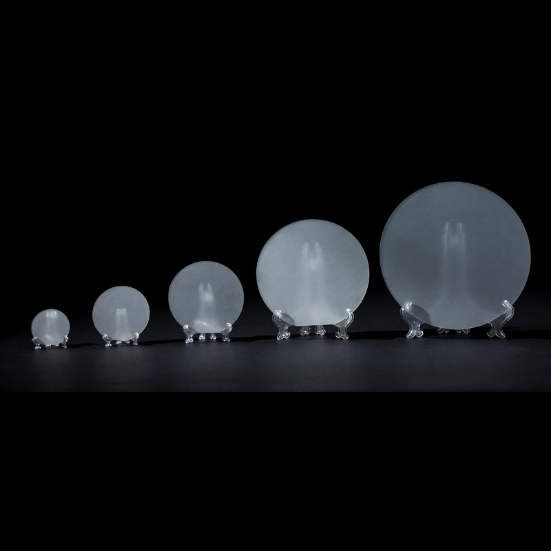
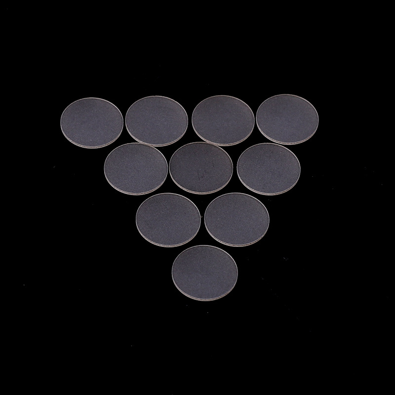
A sapphire substrate is a single-crystal Al₂O₃ wafer used as a base material for growing compound semiconductors like GaN and AlN. It provides high thermal conductivity, chemical stability, and optical transparency, making it essential for LED, LD, and optical coating applications.
Sapphire Substrate Benefits
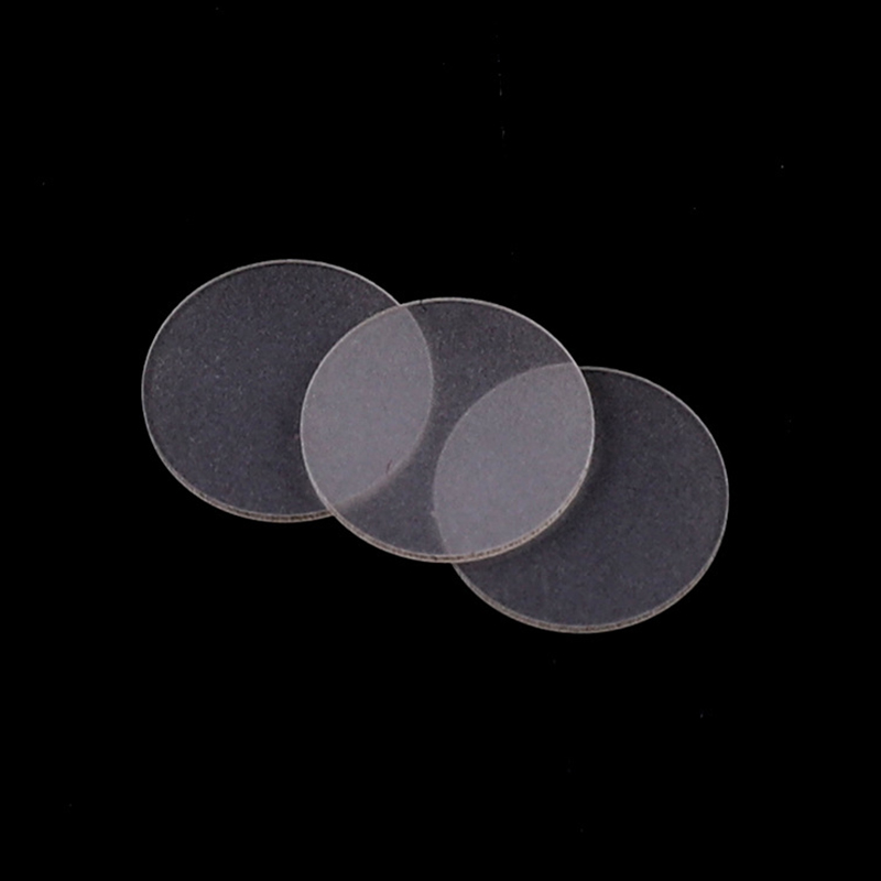
- Epi-ready surface options: single- or double-side epi-polished finishes to support GaN growth and minimize nucleation defects.
- Orientation control: choice of c-plane, m-plane, or r-plane to match device design and crystal growth requirements.
- Dimensional range: stocked standard diameters with custom cutting to match tool pockets and fixture footprints.
- Low intrinsic defect options: material grades and process options that reduce dislocation density for improved epitaxial yield.
Sapphire Substrate Properties
| Property | Value |
| Material | Al2O3 (monocrystalline structure) |
| Purity | 99.999% |
| Max. Working Temperature | 1950℃ |
| Transmissivity | >86% (280-3500nm) |
| Refractive Index (λ ≈ 546 nm) | 1.76 |
| Density | 3.98-4.1g/cm3 |
| Hardness | 1700Hv |
| Compressive Strength | 2100MPa |
| Tensile Strength | 200MPa |
| Bending Strength | 445MPa |
| Elasticity Modulus | 380GPa |
| Poisson's Ratio | 0.28 |
| Thermal Conductivity | 28-32W/m*K |
| Thermal Expansion Coefficient | 6*10-6/K |
| Refractive Index | 1.76 |
| Volume Resistivity | >1.5*1016Ohm*cm |
| Dielectric Strength | 48KV/mm |
| Lattice Constant (a, c) | a = 4.758 Å, c = 12.991 Å |
| Double-Side Polished Surface | Ra < 0.5 nm |
| Decomposition Point | > 2000 °C (in air) |
Sapphire Substrate Specifications
| C-Plane(0001) Sapphire Substrate | |||||
| Item NO. | Inch | Diameter (mm) | Thickness (μm) | TTV/Bow/Warp | Purity |
| AT-BS-JP1001 | 1 Inch | 25.4±0.1 | 430±25 | TTV < 5 μm Bow < 5 μm Warp < 5 μm | 99.999% |
| AT-BS-JP1002 | 2 Inch | 50.8±0.1 | 430±25 | TTV < 10 μm Bow < 10 μmWarp < 10 μm | 99.999% |
| AT-BS-JP1003 | 3 Inch | 76.2±0.1 | 500±25 | TTV < 15 μm Bow < 15 μmWarp < 15 μm | 99.999% |
| AT-BS-JP1004 | 4 Inch | 100±0.1 | 650±25 | TTV < 20 μm Bow < 20 μmWarp < 20 μm | 99.999% |
| AT-BS-JP1005 | 5 Inch | 125±0.1 | 650±25 | TTV < 20 μm Bow < 20 μmWarp < 20 μm | 99.999% |
| AT-BS-JP1006 | 6 Inch | 150±0.2 | 1300±25 | TTV < 25 μm Bow < 25 μmWarp < 25 μm | 99.999% |
| AT-BS-JP1007 | 8 Inch | 200±0.2 | 1300±25 | TTV < 30 μm Bow < 30 μmWarp < 30 μm | 99.999% |
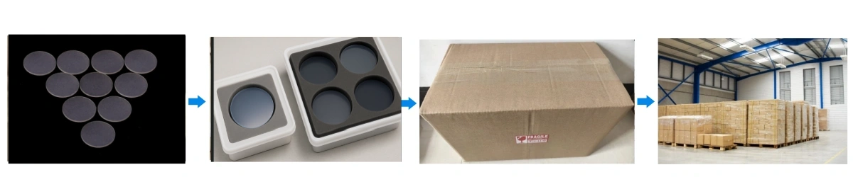
Sapphire Substrate Packaging
- Individual protective carrier (foam or clean plastic carrier) for each wafer.
- Batch trays with vacuum foam inserts for mixed size orders.