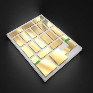
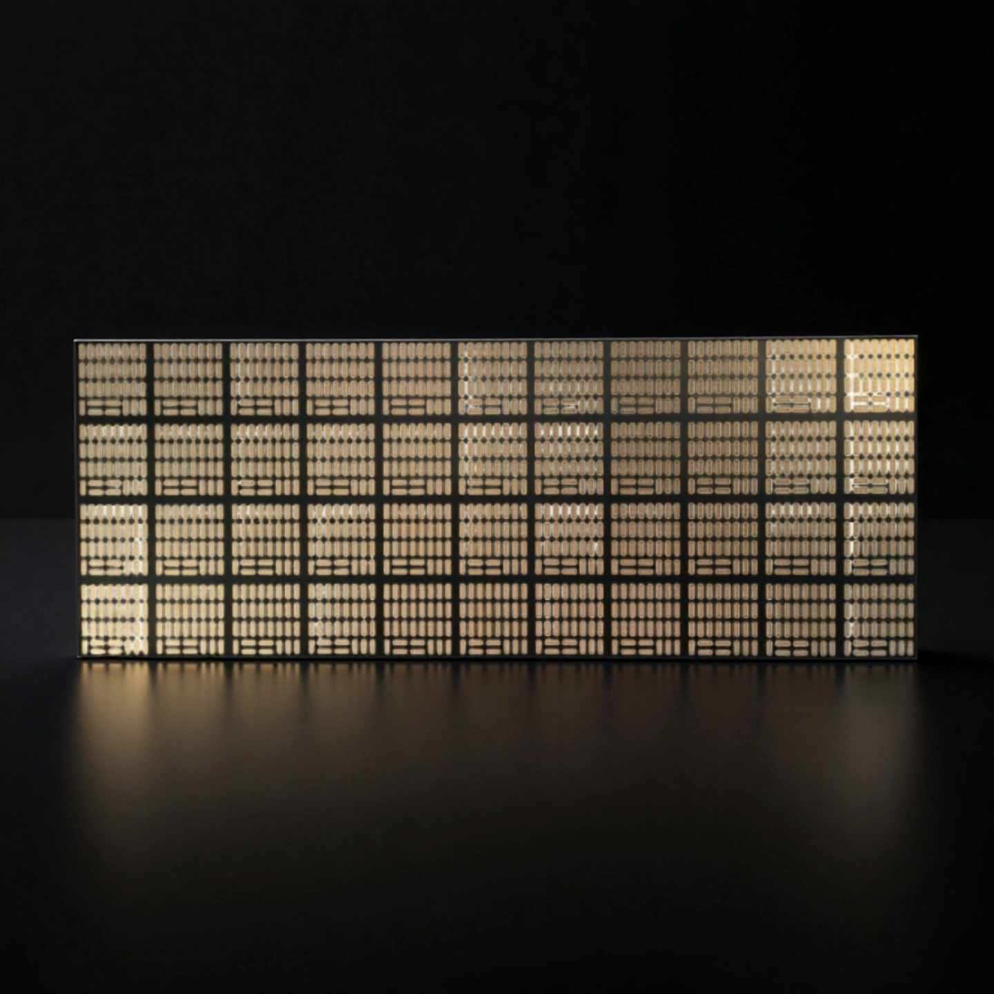
Alumina Metalized Ceramic Substrate for Power Electronics and RF Applications

Our alumina metalized ceramic substrates provide superior thermal management and electrical isolation for high-reliability electronics. Available with 96% or 99.6% Al₂O₃, these substrates are engineered for power modules, RF circuits, and automotive sensors. We offer full customization of metallization patterns (DPC, DBC, Thick Film) to your exact design specifications.

Catalog No. AT-DBC-C001
Material ≥ 96% Al2O3
Dielectric Strength ≥20 kV/mm
Flatness Tolerance ±0.1 mm
Dimensions/Sizes Download PDF
Engineering RFQ Review
Small-Batch Custom Support
Factory-Direct Manufacturing
Drawing & Process Review

Metalized alumina substrate is a high-performance electronic component made from a small, flat alumina ceramic tile. Alumina is a hard electrical insulator with useful thermal conductivity. A patterned metal layer, usually copper, is bonded to its surface to form conductive paths similar to those on a conventional circuit board.

Alumina Metalized Ceramic Substrate Benefits

  • Effective thermal management — 96% or 99.6% alumina (Al₂O₃) conducts heat away from components such as IGBTs and LEDs. Actual thermal performance depends on the substrate design, metallization and heat-sink path.
  • Stable electrical isolation — High dielectric strength and low dielectric loss support high-voltage isolation and signal integrity in high-frequency RF circuits.
  • Metallization adhesion — DBC, DPC and thick-film processes bond copper or refractory-metal layers to the ceramic. Bond strength and thermal-cycling behavior depend on the selected process and design.
  • Precision patterning — Laser processing and photolithography support fine circuit traces and spacing down to approximately 30 µm, depending on the process and design.

Metalized Alumina Substrate Properties

Property Unit 96% Al₂O₃ 99% Al₂O₃ 99.5% Al₂O₃ 99.6% Al₂O₃ 99.7% Al₂O₃ 99.8% Al₂O₃ 99.9% Al₂O₃ 99.99% Al₂O₃
Alumina content % 96 99 99.5 99.6 99.7 99.8 99.9 99.99
Density g/cm³ 3.6-3.75 3.83 3.89 3.91 3.92 3.93 3.94 3.98
Color white Ivory Ivory Ivory Ivory Ivory Ivory Ivory
Water absorption % 0 0 0 0 0 0 0
Young’s modulus (Elastic modulus) GPa 300 350 375 356 357 358 359 362
Shear modulus GPa 152
Bulk modulus GPa 228
Poisson’s ratio 0.22
Compressive strength MPa 1910 2210 2500 2552 2554 2556 2558 2570
Flexural strength MPa 260 300 340 345 346 347 348 365
Fracture toughness MPa·m¹ᐟ² 4
Hardness GPa 14.5 17 17 23 24 25 26 30
Thermal conductivity W/m·K 20 31 31 31-33 31-33 31-33 31-35 31-35
Thermal shock resistance ΔT °C 222 223 224 225 228
Maximum use temperature (no load) °C 1450 1680 ≤1750 1755 1760 1765 1770 1800
Coefficient of thermal expansion 10⁻⁶/°C 7.6 7.6 7.6 7.6 7.5 7.5 7.4 7.4
Volume resistivity Ω·cm >1×10¹⁴ >1×10¹⁴ >1×10¹⁴ >1×10¹⁴ >1×10¹⁴ >1×10¹⁴ >1×10¹⁴ >1×10¹⁴
Dielectric constant (relative permittivity) 9.2 9.5 9.8 9.83 9.84 9.85 9.86 9.92
Dielectric strength kV/mm 15 19 16.9 23.2 23.4 23.6 23.8 24
Dissipation factor (loss factor @ 1 kHz) 0.0002

Al₂O₃ Metalized Ceramic Substrate Specifications

Type 1: Rectangular Alumina Metalized Ceramic Substrate

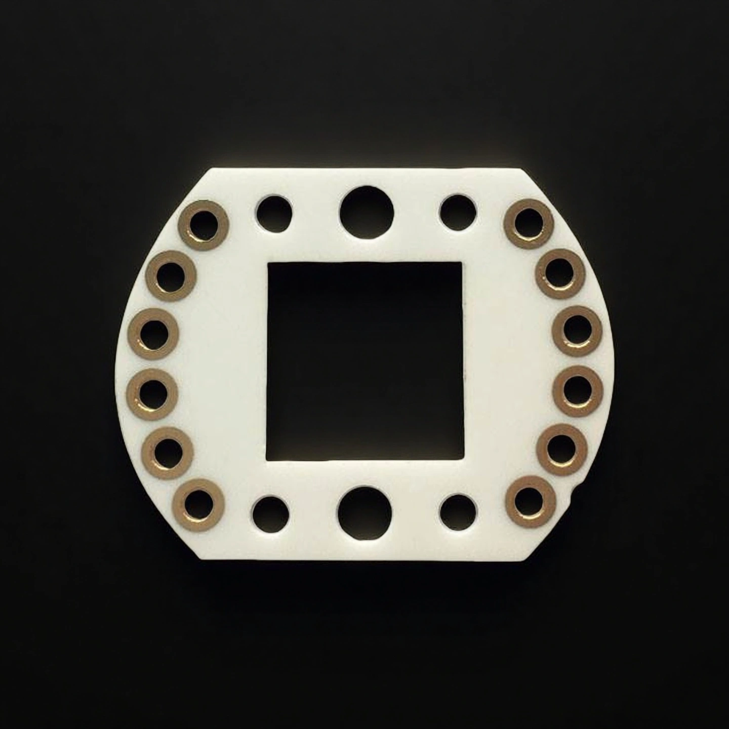
Top view of a rectangular alumina metalized ceramic substrate

Rectangle Alumina Metalized Ceramic Substrate
Item No. Length(mm) Width(mm) Thickness(mm) Copper foil thickness (mm) Copper clad thickness(mm) Purity(%)
AT-DBC-C001 10 5 0.25 0.1-0.6 0.075-0.1 96-99.7
AT-DBC-C002 18 11 0.25 0.1-0.6 0.075-0.1 96-99.7
AT-DBC-C003 20 15 0.38 0.1-0.6 0.075-0.1 96-99.7
AT-DBC-C004 28 9 0.635 0.1-0.6 0.075-0.1 96-99.7
AT-DBC-C005 32 24 0.55 0.1-0.6 0.075-0.1 96-99.7
AT-DBC-C006 55 30 6 0.1-0.6 0.035 96
AT-DBC-C007 70 52 0.76 0.1-0.6 0.075-0.1 96-99.7
AT-DBC-C008 84 35 1 0.1-0.6 0.075-0.1 96-99.7
AT-DBC-C009 103 90 0.635 0.1-0.6 0.075-0.1 96-99.7
AT-DBC-C010 127 105 2 0.1-0.6 0.075-0.1 96-99.7
AT-DBC-C011 156 84 3 0.1-0.6 0.075-0.1 96-99.7
AT-DBC-C012 178 138 5 0.1-0.6 0.075-0.1 96-99.7
AT-DBC-C013 188 138 4.6 0.1-0.6 0.075-0.1 96-99.7

Type 2: Square Alumina Metalized Ceramic Substrate
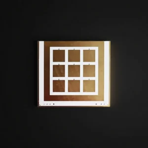
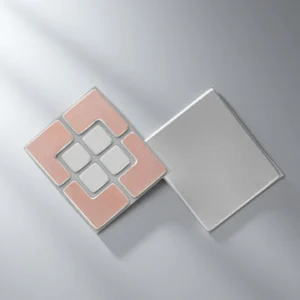
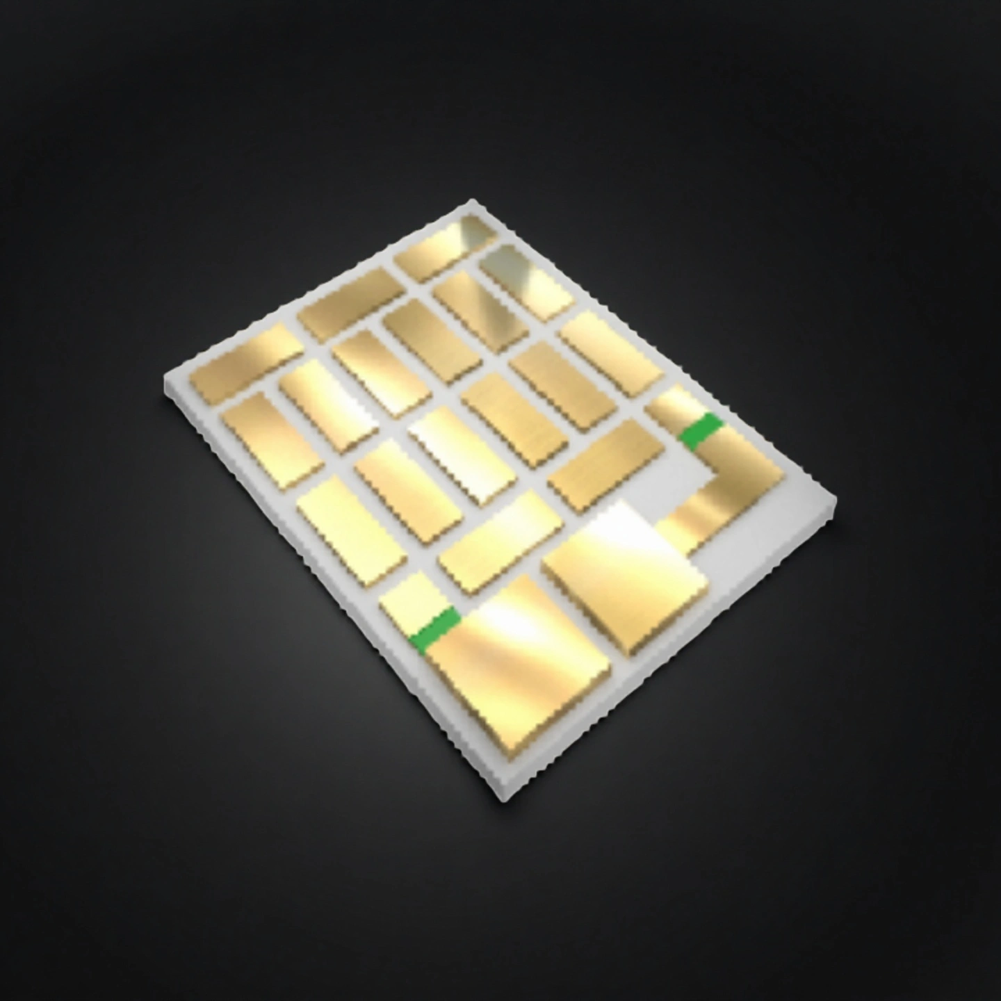
Detailed MoMn coating on an alumina ceramic substrate

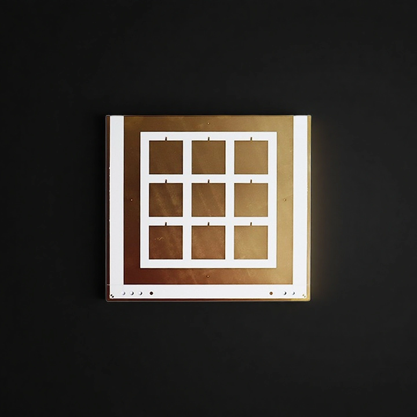
Square Alumina Metalized Ceramic Substrate
Item No. Length(mm) Width(mm) Thickness(mm) Copper foil thickness (mm) Copper clad thickness(mm) Purity(%)
AT-DBC-Z001 10 10 0.25 0.1-0.6 0.075-0.1 96-99.7
AT-DBC-Z002 15 15 0.25 0.1-0.6 0.075-0.1 96-99.7
AT-DBC-Z003 18 18 0.25 0.1-0.6 0.075-0.1 96-99.7
AT-DBC-Z004 25 25 0.38 0.1-0.6 0.075-0.1 96-99.7
AT-DBC-Z005 31.5 31.5 0.635 0.1-0.6 0.075-0.1 96-99.7
AT-DBC-Z006 33 33 0.76 0.1-0.6 0.075-0.1 96-99.7
AT-DBC-Z007 40 40 0.76 0.1-0.6 0.075-0.1 96-99.7
AT-DBC-Z008 60 60 1 0.1-0.6 0.075-0.1 96-99.7
AT-DBC-Z009 72 72 1 0.1-0.6 0.075-0.1 96-99.7
AT-DBC-Z010 100 100 3 0.1-0.6 0.075-0.1 96-99.7
AT-DBC-Z011 127 127 1 0.1-0.6 0.035 99.7
AT-DBC-Z012 138 138 5 0.1-0.6 0.075-0.1 96-99.7

Metalized Alumina Substrate Packaging

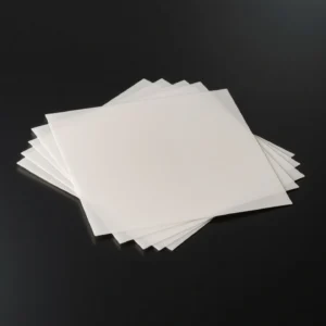
  • Each metalized ceramic substrate is sealed and placed in an anti-static tray with moisture-resistant packaging. Shock-resistant outer cartons protect the parts during transport.
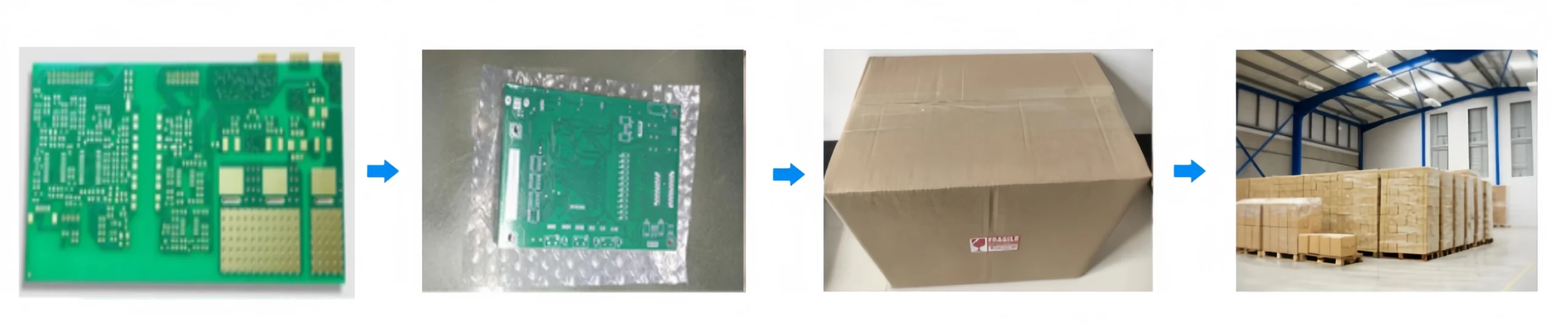
Metalized alumina substrates in protective packaging

Applications for Metallized Alumina Ceramic Substrates

Metallized alumina substrates combine electrical insulation with patterned metal surfaces for current conduction, heat spreading and joining. The appropriate ceramic thickness, metallization route and surface finish should be selected according to the drawing, assembly process and operating requirements.

  • Power Modules, Inverters & Power Supplies

    Engineering need
    Electrically isolate semiconductor devices while carrying current and transferring heat toward the baseplate or cooling interface.

    How the substrate supports the design
    Alumina provides the insulating ceramic base, while the copper or metallized pattern provides conductive, attachment and heat-spreading surfaces.

  • LED, Laser-Diode & Electronic Packages

    Engineering need
    Combine an electrically insulating base with patterned metal features and a surface finish compatible with die attach, soldering or wire bonding.

    How the substrate supports the design
    The alumina ceramic provides electrical isolation and dimensional stability, while the metallization defines the circuit and assembly interfaces.

  • Thermoelectric & Peltier Modules

    Engineering need
    Provide insulated connection surfaces and a controlled interface for module assembly and operation.

    How the substrate supports the design
    Patterned metallization creates the required electrical connection areas, while alumina provides ceramic support and electrical separation.

  • Brazed & Hermetic Ceramic-to-Metal Assemblies

    Engineering need
    Create a controlled, finish-ready metallized interface for brazing or another specified ceramic-to-metal joining process.

    How the substrate supports the design
    Mo-Mn or tungsten thick-film metallization with a reviewed plating system can provide a joining surface matched to the assembly design.

Metalized Alumina Substrate Usage Instructions

  • Receiving and Storage

    1. Inspection: Check the protective packaging and substrates for damage, contamination, edge chips, or coating defects upon receipt.
    2. Storage: Keep substrates in their original clean packaging in a dry, controlled environment.
    3. Contamination Control: Keep them away from dust, moisture, sulfur compounds, and corrosive chemicals that may affect the metal finish.
    4. Storage Period: Follow the confirmed storage limits for the specified surface finish and assembly process.

  • Handling and Preparation

    1. Handling: Hold substrates by the edges using powder-free gloves or finger cots.
    2. Mechanical Protection: Do not bend, drop, or place heavy objects on the substrates. Use suitable padded trays during handling and transport.
    3. Cleaning: Use only a cleaning or bake-out process approved for the selected metallization, surface finish, and assembly method.

  • Assembly and Soldering

    1. Material Application: Use solder paste, braze material, or bonding materials compatible with the specified surface finish and assembly design.
    2. Component Placement: Control placement force to prevent ceramic cracking, edge damage, or metallization damage.
    3. Thermal Profile: Establish and validate the preheating, joining, and cooling profile according to the assembly materials, substrate stack-up, and equipment.

  • Post-Assembly Cleaning and Inspection

    1. Cleaning: Follow the flux or bonding-material supplier’s recommended cleaning process. Avoid aggressive ultrasonic cleaning unless it has been validated for the assembly.

    2. Inspection: Check the joints, component alignment, metallized surfaces, edges, and corners according to the approved drawing and quality plan.

Metalized Alumina Substrate FAQ

  1. Q: Is the alumina dielectric-strength value enough to confirm the working voltage?
    A: No. Dielectric strength describes the ceramic material under specified test conditions, not the voltage rating of the finished module. Ceramic thickness, conductor spacing, pattern geometry, surface condition, operating environment and test method must also be reviewed.
  2. Q: How is the maximum operating temperature determined?
    A: There is no single temperature rating for every metallized alumina substrate. The practical limit depends on the ceramic, metallization route, surface finish, joining system, attached components, exposure time and thermal-cycle conditions.
  3. Q: What can cause the metal layer to separate from the ceramic?
    A: Possible causes include surface contamination, unsuitable metallization, excessive thermal or mechanical stress, poorly designed metal geometry and an assembly process that does not match the substrate stack-up. Project-specific process validation is required.
  4. Q: How should thermal-cycling requirements be specified?
    A: Please define the minimum and maximum temperatures, ramp rate, dwell time, required cycle count, mounting condition, cooling interface and acceptance criteria. Power cycling and environmental cycling should be identified separately.
  5. Q: How should the surface finish be selected?
    A: The finish must match the downstream joining process. Bare copper, nickel, nickel/gold or silver may be considered depending on whether the substrate will be soldered, brazed or wire-bonded.
  6. Q: Can partial or patterned metallization be requested?
    A: Yes. Partial or patterned metallization can be evaluated from a drawing showing the coated areas, keep-out zones, pattern dimensions, alignment requirements, metal thickness and surface finish. Final manufacturability is confirmed during drawing review.
  7. Q: Can ADCERAX evaluate an existing substrate as a second-source option?
    A: Yes. ADCERAX can review the existing drawing, ceramic grade, layer stack-up, metallization route, finish and qualification requirements. The proposed alternative must be evaluated and validated before production approval.
  8. Q: Are ceramic-body properties the same as finished-substrate properties?
    A: No. Density, dielectric strength, thermal expansion and thermal conductivity describe the ceramic body. Metal thickness, adhesion, pattern accuracy and surface finish describe the metallization system. Finished performance also depends on the interfaces, geometry and assembly conditions.
  9. Q: How are tolerances and acceptance criteria confirmed?
    A: Critical dimensions, pattern registration, flatness, edge condition, metal thickness, surface finish and required tests should be defined in the approved drawing or quality document before production.
  10. Q: What should be controlled when moving from prototypes to repeat production?
    A: The approved drawing revision, ceramic grade, metallization process, layer thicknesses, surface finish, critical dimensions, inspection criteria and packaging requirements should be fixed before repeat production. Any material, process or design change should be reviewed before implementation.
customize size

Customize Alumina Metalized Substrates

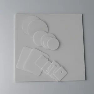
We manufacture alumina metalized substrates according to your engineering drawings and application requirements. The following parameters can be customized:

  • Material: Alumina (Al₂O₃) purity from 96% to 99.7%.
  • Dimensions: Custom shapes and sizes with dimensional tolerances as tight as ±0.05 mm.
  • Thickness: Substrate thickness from 0.25 mm to 2.0 mm.
  • Metallization process: Direct Bonded Copper (DBC), Direct Plated Copper (DPC), or thick-film metallization using Mo/Mn or tungsten.
  • Metallization layers: Copper thickness from 18 µm to 300 µm, with optional nickel, gold, or silver plating.
  • Features: Laser-drilled vias, castellations, scored break lines, and laser-etched part numbers.
  • Surface finish: As-fired, lapped, or polished surfaces according to the required surface roughness.

Related Products

ADCERAX - Your Trusted Advanced Ceramics Manufacturing Partner

Direct factory manufacturing with comprehensive ceramic materials expertise and global supply capabilities

China-Based Manufacturer

ADCERAX supplies ceramic components for overseas OEMs, equipment builders, and labs.

Custom Drawing Support

We review drawings, dimensions, materials, and application conditions before quotation.

Ceramic Process Control

Forming, sintering, machining, grinding, and finishing are arranged by part requirements.

Pre-Shipment Inspection

Dimensional checks, visual inspection, and packaging review help reduce procurement risk.

Get in Touch with Us

Our team will be happy to respond to you in less than 24 hours.

Pingxiang Factory — Silicon carbide, silicon nitride, high-temperature ceramics

Quick Quotation

*Our team will answer your inquiries within 24 hours.

*Your information will be kept strictly confidential.

Ready to Solve Your Engineering Challenge?

Partner with ADCERAX for reliable, high-performance advanced ceramic solutions. Our engineers are ready to discuss your project.

E-mail

info@adcerax.com

Phone

Tel: +86-0731-84428843 WhatsApp: +86 19311583352

Response Time

Within 24 hours

Quick Quote

The more details you provide, the faster we can quote.

*We respond within 24 hours. All inquiries are confidential.

Get Your Custom Solution

The more details you provide, the faster we can respond.

customize size

*We respond within 24 hours. All inquiries are confidential.

Download Catalog