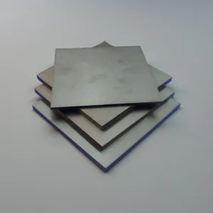

A high purity alumina ceramic substrate is a dense Al₂O₃ ceramic plate used as an electrically insulating and thermally stable base for electronic circuits, LED packages, sensors and RF modules. Compared with polymer circuit boards, alumina provides better heat resistance, dielectric strength, dimensional stability and surface durability. The final grade, thickness, surface finish and hole layout should be selected according to the circuit type, assembly process and operating environment.
Why Engineers Choose Alumina Ceramic Substrates
Alumina ceramic substrates are selected when an electronic assembly needs reliable insulation, stable ceramic performance and controlled surface quality. Compared with polymer boards or metal carriers, dense Al₂O₃ substrates can provide better resistance to heat, voltage, dimensional drift and surface wear in demanding circuit and module designs.
Electrical Insulation
Dense Al₂O₃ provides high dielectric strength and stable volume resistivity. This helps isolate circuits, sensors and power devices from unwanted current paths, especially in assemblies where voltage stability and insulation reliability are important.
Heat Resistance
Alumina keeps mechanical and electrical stability under elevated temperatures. This makes it suitable for substrates exposed to soldering, firing, curing, bonding or repeated thermal cycling during production and service.
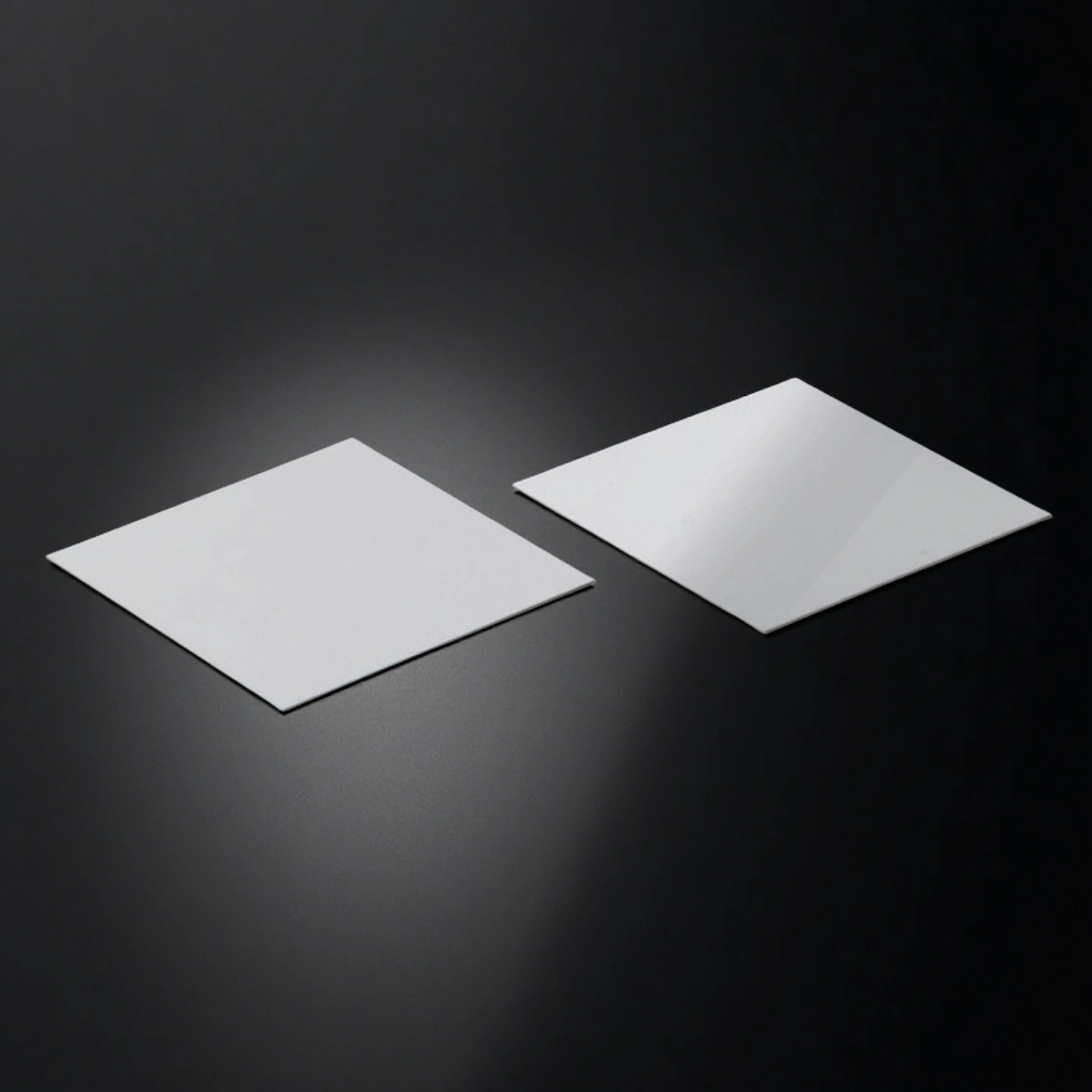
Surface Control
As-fired, fine-ground, lapped and polished surfaces can be selected according to the circuit process. Surface finish affects metallization, bonding, thin-film uniformity and final circuit reliability, so it should be matched to the application instead of selected only by cost.
Dimensional Stability
Alumina has a stable ceramic structure and controlled thermal expansion. This helps reduce warpage, alignment drift and assembly stress when the substrate is used in precision electronic, sensor or module structures.
Machining Flexibility
Holes, slots, scribing lines and custom outlines can be reviewed by drawing. This allows the alumina substrate to match the circuit layout, mounting position or mechanical interface more accurately before production.
Typical Properties for Alumina Ceramic Substrate Selection
| Property | Typical Range / Option | Selection Note |
|---|---|---|
| Alumina purity | 96%, 99%, 99.5%, 99.6%, 99.8% | 96% is often used for general thick-film and insulation parts, while 99.6% or higher is preferred for finer surface and lower dielectric loss requirements. |
| Thermal conductivity | About 20–35 W/m·K, depending on grade and test condition. | Alumina provides better thermal stability than many organic boards, but AlN should be considered when very high heat spreading is required. |
| Dielectric strength | Grade and thickness dependent. | This parameter should be confirmed according to operating voltage, substrate thickness and edge design. |
| Surface finish | As-fired, fine-ground, lapped or polished. | Polished surfaces are preferred for thin-film, RF and precision bonding applications. |
| Thickness range | Thin sheet to thicker ceramic plate options. | Thin substrates need careful handling and packaging to avoid edge chipping or cracking. |
| Processing options | Laser drilling, laser scribing, cutting, grinding and polishing. | Hole diameter, pitch, edge distance and thickness must be reviewed together. |
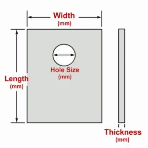
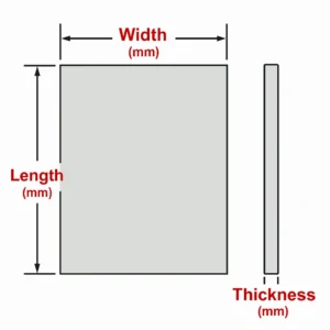
Size, Thickness and Processing Options
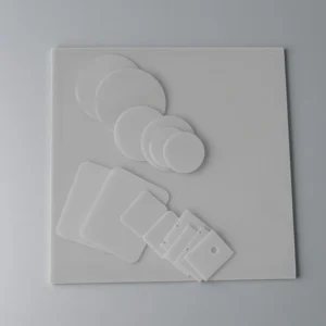
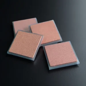
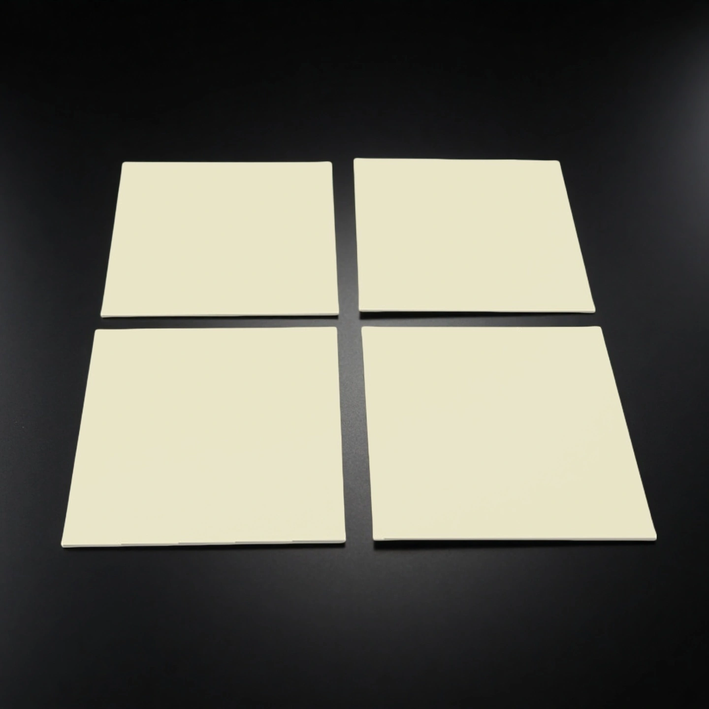
ADCERAX can supply alumina ceramic substrates in square, rectangular, round and drawing-based shapes. Standard sizes are suitable for prototype evaluation, circuit testing and small-batch assembly, while custom substrates can be reviewed according to circuit layout, hole position, scribing line, surface finish and thickness tolerance.
Type 1-96 Alumina Substrate Rectangular with Hole
| Item NO. | L* W*Thickness (mm) | Hole Dia (mm) |
| TE-J-1 | 10*2.4*2 | \ |
| TE-J-2 | 10*2.4*1.5 | \ |
| TE-J-3 | 10*15*0.6 | 4 |
| TE-J-4 | 10*16*1.5 | 3.5 |
| TE-J-5 | 10*20*1.6 | \ |
| TE-J-6 | 10*16*6 | \ |
| TE-J-7 | 10*10*2 | \ |
| TE-J-8 | 10*14*2 | \ |
| TE-J-9 | 10.4*18*1 | 3.8 |
| TE-J-10 | 10.6*17*1 | 3.8 |
| TE-J-11 | 11*11*1 | \ |
| TE-J-12 | 11*17*1 | \ |
| TE-J-13 | 11*7*1.5 | \ |
| TE-J-14 | 11*18*1 | 4 |
| TE-J-15 | 12*18.5*0.6 | 3.8 |
| TE-J-16 | 12*18*0.6 | 3.8 |
| TE-J-17 | 12*18.5*1 | \ |
| TE-J-18 | 12*18.5*0.6 | \ |
| TE-J-19 | 12.7*16.5*1.8 | 3.8 |
| TE-J-20 | 13*19*0.6 | \ |
| TE-J-21 | 14*18*3 | 3.4 |
| TE-J-22 | 14*19*2 | 3.5 |
| TE-J-23 | 14*20*1 | 3.2/3.5 |
| TE-J-24 | 14*20*0.6 | 3.2 |
| TE-J-25 | 14*20*1 | \ |
| TE-J-26 | 14*20*0.6 | \ |
| TE-J-27 | 14*20*2 | \ |
| TE-J-28 | 14*20*2 | 3.2 |
| TE-J-29 | 15*19.5*1 | 3.8 |
| TE-J-30 | 15*2*2.4 | \ |
| TE-J-31 | 16*21*2.5 | 3.5 |
| TE-J-32 | 16*22*0.6 | 3.3 |
| TE-J-33 | 16*22*0.6 | 4 |
| TE-J-34 | 16*22*0.6 | 3.7 |
| TE-J-35 | 16*46*1 | \ |
| TE-J-36 | 17*22*1 | 3.7 |
| TE-J-37 | 17*22*0.6 | 3.7 |
| TE-J-38 | 17*22*0.6 | \ |
| TE-J-39 | 17*22*1.5 | \ |
| TE-J-40 | 17*22*1 | \ |
| TE-J-41 | 17*37.1*1 | \ |
| TE-J-85 | 22*30*2 | \ |
| TE-J-86 | 22*28*1 | 3.4 |
| TE-J-87 | 22*28*0.6 | 3.4 |
| TE-J-88 | 22*28*1 | \ |
| TE-J-89 | 22*28*0.6 | \ |
| TE-J-90 | 22*25*1 | 3.6 |
| TE-J-91 | 22*25*0.6 | 3.1 |
| TE-J-92 | 22*25*1 | 3.1 |
| TE-J-93 | 22*22*0.6 | 3 |
| TE-J-94 | 22*35*1 | \ |
| TE-J-95 | 22*35*1.5 | 3.5 |
| TE-J-96 | 23*34*1 | 3.2 |
| TE-J-97 | 24*30*1 | \ |
| TE-J-98 | 24*35.5*1 | \ |
| TE-J-99 | 24*40*0.6 | \ |
| TE-J-100 | 24*60*1 | \ |
| TE-J-101 | 24*70*0.6 | \ |
| TE-J-102 | 24*72*1 | \ |
| TE-J-103 | 24*90*0.6 | \ |
| TE-J-104 | 24*95*1 | \ |
| TE-J-105 | 24*125*1 | \ |
| TE-J-106 | 24*104*1 | \ |
| TE-J-107 | 25*34*0.6 | \ |
| TE-J-108 | 25*40*1 | \ |
| TE-J-109 | 25*40*0.6 | \ |
| TE-J-110 | 25*110*0.6 | \ |
| TE-J-111 | 26*30*1 | 3.2 |
| TE-J-112 | 26*31*1 | 3.5 |
| TE-J-113 | 26*35*1 | \ |
| TE-J-114 | 27*60*0.6 | \ |
| TE-J-115 | 27*90*0.6 | \ |
| TE-J-116 | 27*48*1 | 5 |
| TE-J-117 | 27.5*4.2*2.5 | \ |
| TE-J-118 | 28*40*1 | \ |
| TE-J-119 | 28*42*0.6 | \ |
| TE-J-120 | 28*44*0.6 | 6 |
| TE-J-121 | 28*64*1 | \ |
| TE-J-122 | 28*72*1 | \ |
| TE-J-123 | 29*33*1.3 | \ |
| TE-J-124 | 30*38*1 | 3.5 |
| TE-J-125 | 30*40*1 | 3.5 |
| TE-J-126 | 30*43*0.6 | 4.5 |
| TE-J-127 | 32*50*1 | \ |
| TE-J-128 | 32*60*1 | \ |
| TE-J-129 | 33*53*1.3 | \ |
| TE-J-130 | 33*73*1.3 | \ |
| TE-J-131 | 33.6*51.4*0.8 | 5 |
| TE-J-132 | 33.6*51.4*2 | 5 |
| TE-J-133 | 34*64*0.6 | \ |
| TE-J-134 | 34*39*0.6 | \ |
| TE-J-135 | 35*48*1 | 5.5 |
| TE-J-136 | 35*68*1 | \ |
| TE-J-137 | 35*45*1 | \ |
| TE-J-138 | 35*85*0.6 | \ |
| TE-J-139 | 38*38*0.6 | \ |
| TE-J-140 | 38*50*0.6 | \ |
| TE-J-141 | 35*35*20 | \ |
| TE-J-142 | 38.5*41*1 | \ |
| TE-J-143 | 39*91*0.6 | \ |
| TE-J-144 | 40*30*1 | 3.5 |
| TE-J-145 | 40*56*1 | \ |
| TE-J-146 | 40*43*0.6 | \ |
| TE-J-147 | 40*105*0.635 | \ |
| TE-J-148 | 40*140*0.6 | \ |
| TE-J-149 | 40*150*1 | \ |
| TE-J-150 | 40*260*1 | \ |
| TE-J-151 | 44*16*1 | \ |
| TE-J-152 | 44*28*0.6 | 6 |
| TE-J-153 | 50*50*1 | \ |
| TE-J-154 | 50*50*3 | \ |
| TE-J-155 | 55*18*2 | \ |
| TE-J-156 | 75*18*2 | \ |
| TE-J-157 | 100*100*1 | \ |
| TE-J-158 | 100*100*2 | \ |
| TE-J-159 | 100*100*3 | \ |
| TE-J-160 | 120*160*2 | \ |
| TE-J-161 | 120*160*3 | \ |
| TE-J-162 | 120*160*4 | \ |
| TE-J-163 | 120*160*6 | \ |
| TE-J-164 | 160*160*1 | \ |
| TE-J-165 | 160*160*0.6 | \ |
Type 2-96 Alumina Substrate Rectangular
| Item | Length(mm) | Width(mm) | Thickness(mm) | Purity(%) |
| TE-J-169 | 10 | 10 | 0.25 | 96-99.8% |
| TE-J-170 | 10 | 10 | 0.5 | 96-99.8% |
| TE-J-171 | 10 | 10 | 0.635 | 96-99.8% |
| TE-J-172 | 10 | 10 | 1 | 96-99.8% |
| TE-J-173 | 20 | 20 | 1 | 96-99.8% |
| TE-J-174 | 20 | 20 | 2 | 96-99.8% |
| TE-J-175 | 25 | 25 | 1 | 96-99.8% |
| TE-J-176 | 30 | 30 | 0.635 | 96-99.8% |
| TE-J-177 | 30 | 30 | 1 | 96-99.8% |
| TE-J-178 | 30 | 30 | 2 | 96-99.8% |
| TE-J-179 | 35 | 35 | 1 | 96-99.8% |
| TE-J-180 | 40 | 40 | 1 | 96-99.8% |
| TE-J-181 | 40 | 40 | 5 | 96-99.8% |
| TE-J-182 | 50 | 50 | 0.5 | 96-99.8% |
| TE-J-183 | 50 | 50 | 0.635 | 96-99.8% |
| TE-J-184 | 50 | 50 | 1.5 | 96-99.8% |
| TE-J-185 | 50 | 50 | 5 | 96-99.8% |
| TE-J-191 | 60 | 60 | 1 | 96-99.8% |
| TE-J-192 | 65 | 74 | 0.2 | 96-99.8% |
| TE-J-193 | 65 | 74 | 0.28 | 96-99.8% |
| TE-J-194 | 70 | 70 | 2 | 96-99.8% |
| TE-J-195 | 70 | 70 | 3 | 96-99.8% |
| TE-J-196 | 76.2 | 76.2 | 0.75 | 96-99.8% |
| TE-J-197 | 80 | 80 | 3 | 96-99.8% |
| TE-J-198 | 80 | 80 | 5 | 96-99.8% |
| TE-J-199 | 80 | 110 | 5 | 96-99.8% |
| TE-J-200 | 84 | 84 | 0.8 | 96-99.8% |
| TE-J-201 | 100 | 100 | 0.5 | 96-99.8% |
| TE-J-202 | 100 | 100 | 0.635 | 96-99.8% |
| TE-J-203 | 100 | 100 | 1.2 | 96-99.8% |
| TE-J-204 | 100 | 100 | 1.5 | 96-99.8% |
| TE-J-205 | 100 | 100 | 2.2 | 96-99.8% |
| TE-J-206 | 100 | 100 | 2.5 | 96-99.8% |
| TE-J-207 | 100 | 100 | 3.5 | 96-99.8% |
| TE-J-208 | 100 | 100 | 0.25 | 96-99.8% |
| TE-J-209 | 100 | 100 | 1.055 | 96-99.8% |
| TE-J-210 | 100 | 100 | 0.25 | 96-99.8% |
| TE-J-211 | 100 | 100 | 0.35 | 96-99.8% |
| TE-J-212 | 100 | 100 | 0.5 | 96-99.8% |
| TE-J-213 | 100 | 100 | 0.6 | 96-99.8% |
| TE-J-214 | 100 | 100 | 0.7 | 96-99.8% |
| TE-J-215 | 100 | 100 | 1.5 | 96-99.8% |
| TE-J-216 | 100 | 100 | 2.335 | 96-99.8% |
| TE-J-217 | 100 | 100 | 2.5 | 96-99.8% |
| TE-J-218 | 100 | 100 | 3.2 | 96-99.8% |
| TE-J-219 | 100 | 100 | 3.5 | 96-99.8% |
| TE-J-220 | 100 | 100 | 4 | 96-99.8% |
| TE-J-221 | 100 | 100 | 5 | 96-99.8% |
| TE-J-227 | 109 | 109 | 1 | 96-99.8% |
| TE-J-228 | 110 | 110 | 5 | 96-99.8% |
| TE-J-229 | 114 | 114 | 1 | 96-99.8% |
| TE-J-230 | 114 | 114 | 0.38 | 96-99.8% |
| TE-J-231 | 114 | 114 | 0.5 | 96-99.8% |
| TE-J-232 | 114 | 114 | 0.65 | 96-99.8% |
| TE-J-233 | 115 | 115 | 0.12 | 96-99.8% |
| TE-J-234 | 115 | 115 | 0.125 | 96-99.8% |
| TE-J-235 | 120 | 120 | 0.25 | 96-99.8% |
| TE-J-236 | 120 | 120 | 0.38 | 96-99.8% |
| TE-J-237 | 120 | 120 | 0.5 | 96-99.8% |
| TE-J-238 | 120 | 120 | 0.635 | 96-99.8% |
| TE-J-239 | 120 | 120 | 0.8 | 96-99.8% |
| TE-J-240 | 120 | 120 | 0.25 | 96-99.8% |
| TE-J-241 | 120 | 120 | 1 | 96-99.8% |
| TE-J-242 | 120 | 120 | 3 | 96-99.8% |
| TE-J-243 | 125 | 125 | 2 | 96-99.8% |
| TE-J-244 | 127 | 127 | 1 | 96-99.8% |
| TE-J-245 | 127 | 127 | 1.5 | 96-99.8% |
| TE-J-246 | 138 | 190 | 0.25 | 96-99.8% |
| TE-J-247 | 138 | 190 | 0.38 | 96-99.8% |
| TE-J-248 | 138 | 190 | 0.32 | 96-99.8% |
| TE-J-249 | 138 | 190 | 0.5 | 96-99.8% |
| TE-J-250 | 138 | 190 | 0.8 | 96-99.8% |
| TE-J-251 | 138 | 190 | 0.65 | 96-99.8% |
| TE-J-252 | 138 | 190 | 1 | 96-99.8% |
| TE-J-253 | 138 | 190 | 0.38 | 96-99.8% |
| TE-J-254 | 138 | 190 | 0.5 | 96-99.8% |
| TE-J-255 | 138 | 190 | 0.635 | 96-99.8% |
| TE-J-256 | 138 | 190 | 1 | 96-99.8% |
| TE-J-257 | 150 | 150 | 1.8 | 96-99.8% |
| TE-J-258 | 150 | 150 | 1 | 96-99.8% |
| TE-J-259 | 150 | 150 | 1.5 | 96-99.8% |
| TE-J-260 | 150 | 150 | 2 | 96-99.8% |
| TE-J-261 | 150 | 150 | 3 | 96-99.8% |
| TE-J-262 | 150 | 150 | 5 | 96-99.8% |
| TE-J-263 | 150 | 150 | 8 | 96-99.8% |
| TE-J-264 | 152 | 152 | 0.635 | 96-99.8% |
| TE-J-265 | 160 | 170 | 2.5 | 96-99.8% |
| TE-J-266 | 180 | 180 | 2 | 96-99.8% |
| TE-J-267 | 180 | 180 | 3 | 96-99.8% |
| TE-J-268 | 180 | 180 | 5 | 96-99.8% |
| TE-J-269 | 200 | 200 | 2 | 96-99.8% |
| TE-J-270 | 200 | 200 | 3 | 96-99.8% |
| TE-J-271 | 200 | 200 | 5 | 96-99.8% |
| TE-J-272 | 220 | 220 | 2 | 96-99.8% |
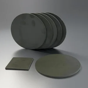
Type 3-96 Alumina Substrate Round
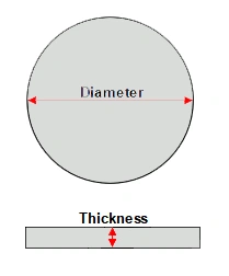
| Item | Diameter(mm) | Thickness(mm) | Purity(%) |
| TE-AD-002 | 3.5 | 1 | 96-99.8% |
| TE-AD-003 | 5 | 1 | 96-99.8% |
| TE-AD-004 | 6 | 0.25 | 96-99.8% |
| TE-AD-005 | 6 | 0.5 | 96-99.8% |
| TE-AD-006 | 6 | 0.635 | 96-99.8% |
| TE-AD-007 | 6 | 1 | 96-99.8% |
| TE-AD-008 | 8 | 0.25 | 96-99.8% |
| TE-AD-009 | 8 | 0.5 | 96-99.8% |
| TE-AD-010 | 8 | 0.635 | 96-99.8% |
| TE-AD-011 | 8 | 1 | 96-99.8% |
| TE-AD-012 | 10 | 0.25 | 96-99.8% |
| TE-AD-013 | 10 | 0.38 | 96-99.8% |
| TE-AD-014 | 10 | 0.5 | 96-99.8% |
| TE-AD-015 | 10 | 0.635 | 96-99.8% |
| TE-AD-016 | 10 | 1 | 96-99.8% |
| TE-AD-017 | 12 | 0.25 | 96-99.8% |
| TE-AD-018 | 12 | 0.5 | 96-99.8% |
| TE-AD-019 | 12 | 0.635 | 96-99.8% |
| TE-AD-020 | 12 | 1 | 96-99.8% |
| TE-AD-021 | 16 | 0.25 | 96-99.8% |
| TE-AD-022 | 16 | 0.5 | 96-99.8% |
| TE-AD-023 | 16 | 0.635 | 96-99.8% |
| TE-AD-024 | 16 | 1 | 96-99.8% |
| TE-AD-025 | 18 | 0.5 | 96-99.8% |
| TE-AD-026 | 18 | 0.635 | 96-99.8% |
| TE-AD-027 | 18 | 1 | 96-99.8% |
| TE-AD-028 | 20 | 0.25 | 96-99.8% |
| TE-AD-029 | 20 | 0.5 | 96-99.8% |
| TE-AD-030 | 20 | 0.635 | 96-99.8% |
| TE-AD-031 | 20 | 1 | 96-99.8% |
| TE-AD-032 | 25 | 0.5 | 96-99.8% |
| TE-AD-033 | 25 | 0.65 | 96-99.8% |
| TE-AD-034 | 25 | 1 | 96-99.8% |
| TE-AD-035 | 30 | 0.5 | 96-99.8% |
| TE-AD-036 | 30 | 0.635 | 96-99.8% |
| TE-AD-037 | 30 | 1 | 96-99.8% |
| TE-AD-038 | 33 | 1 | 96-99.8% |
| TE-AD-039 | 35 | 1 | 96-99.8% |
| TE-AD-040 | 35 | 2 | 96-99.8% |
| TE-AD-041 | 36 | 4 | 96-99.8% |
| TE-AD-042 | 40 | 1 | 96-99.8% |
| TE-AD-043 | 40 | 1.5 | 96-99.8% |
| TE-AD-044 | 42 | 2 | 96-99.8% |
| TE-AD-045 | 50 | 0.5 | 96-99.8% |
| TE-AD-046 | 50 | 0.635 | 96-99.8% |
| TE-AD-047 | 50 | 1 | 96-99.8% |
| TE-AD-048 | 50 | 2 | 96-99.8% |
| TE-AD-049 | 55 | 0.5 | 96-99.8% |
| TE-AD-050 | 60 | 10 | 96-99.8% |
| TE-AD-051 | 65 | 0.5 | 96-99.8% |
| TE-AD-052 | 75 | 1 | 96-99.8% |
| TE-AD-053 | 82 | 6 | 96-99.8% |
| TE-AD-054 | 89 | 5.5 | 96-99.8% |
| TE-AD-055 | 100 | 0.5 | 96-99.8% |
| TE-AD-056 | 100 | 0.635 | 96-99.8% |
| TE-AD-057 | 100 | 1 | 96-99.8% |
| TE-AD-058 | 101.6 | 0.5 | 96-99.8% |
| TE-AD-059 | 101.6 | 1 | 96-99.8% |
| TE-AD-060 | 120 | 2 | 96-99.8% |
| TE-AD-061 | 125 | 6 | 96-99.8% |
Type 4: Alumina ceramic substrate for thin film circuit

| Specification Dimensions | Alumina Ceramic Substrate | |||
|---|---|---|---|---|
| As-fired Wafer | Fine Ground Wafer | Polished Wafer | ||
| Outline Dimensions | Max (mm) | 101.6×101.6 | 101.6×101.6 | 101.6×101.6 |
| Typical (mm) | 50.8×50.8, 76.2×76.2, 101.6×101.6 | 50.8×50.8, 76.2×76.2, 101.6×101.6 | 50.8×50.8, 76.2×76.2, 101.6×101.6 | |
| Tolerance (mm) | Standard Grade: ≤±0.8%, but absolute value ≥±0.1; Precision Grade: ≤±0.5%, but absolute value ≥±0.05; |
Standard Grade: ≤±0.5%, but absolute value ≥±0.08; Precision Grade: ≤±0.2%, but absolute value ≥±0.05; |
Standard Grade: ≤±0.5%, but absolute value ≥±0.08; Precision Grade: ≤±0.2%, but absolute value ≥±0.05; |
|
| Substrate Thickness | Thickness Range (mm) | 0.15~2.5 | 0.15~2.5 | 0.15~2.5 |
| Typical (mm) | 0.150, 0.254, 0.381, 0.508 | 0.150, 0.254, 0.381, 0.508 | 0.150, 0.254, 0.381, 0.508 | |
| Tolerance (mm) | Standard Grade: ≤±10.0%, but absolute value ≥±0.05; Precision Grade: ≤±5.0%, but absolute value ≥±0.02; |
Standard Grade: ≤±5.0%, but absolute value ≥±0.04; Precision Grade: ≤±1.0%, but absolute value ≥±0.02; |
Standard Grade: ≤±5.0%, but absolute value ≥±0.04; Precision Grade: ≤±1.0%, but absolute value ≥±0.02; |
|
| Laser Drilling | Min (mm, recommended 0.8-1.5 times substrate thickness) | Φ0.08 | Φ0.08 | Φ0.08 |
| Laser Drilled Hole Front/Back Aperture Difference | ≤20% | ≤20% | ≤20% | |
| Minimum Hole Pitch (mm, recommended 3 times hole diameter or more) | ≥0.25 | ≥0.25 | ≥0.25 | |
| Warp | mm/mm | 0.005/mm | 0.003/mm | 0.002/mm |
Type 5: 996 Alumina Substrates size
| 996 Alumina Substrates | ||
| Item No. | Thickness(mm) | Length *Width(mm) |
| AT-AO-J1001 | 0.15 | 50.8×50.8 |
| AT-AO-J1002 | 0.254 | |
| AT-AO-J1003 | 0.381 | |
| AT-AO-J1004 | 0.508 | |
| AT-AO-J1005 | 0.635 | |
| AT-AO-J1006 | 1.0 | |
| AT-AO-J1007 | 2.0 | |
| AT-AO-J1008 | 2.5 | |
| AT-AO-J1009 | 0.15 | 76.2×76.2 |
| AT-AO-J1010 | 0.254 | |
| AT-AO-J1011 | 0.381 | |
| AT-AO-J1012 | 0.508 | |
| AT-AO-J1013 | 0.635 | |
| AT-AO-J1014 | 1.0 | |
| AT-AO-J1015 | 2.0 | |
| AT-AO-J1016 | 2.5 | |
| AT-AO-J1017 | 0.15 | 101.6×101.6 |
| AT-AO-J1018 | 0.254 | |
| AT-AO-J1019 | 0.381 | |
| AT-AO-J1020 | 0.508 | |
| AT-AO-J1021 | 0.635 | |
| AT-AO-J1022 | 1.0 | |
| AT-AO-J1023 | 2.0 | |
| AT-AO-J1024 | 2.5 | |
| AT-AO-J1025 | 0.15 | 114.3×114.3 |
| AT-AO-J1026 | 0.254 | |
| AT-AO-J1027 | 0.381 | |
| AT-AO-J1028 | 0.508 | |
| AT-AO-J1029 | 0.635 | |
| AT-AO-J1030 | 1.0 | |
| AT-AO-J1031 | 2.0 | |
| AT-AO-J1032 | 2.5 | |
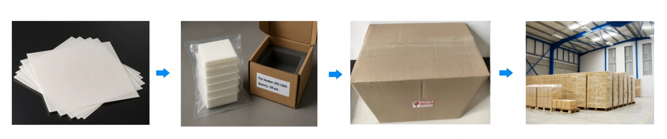
High Purity Alumina Substrates Packaging
- Substrates are separated by soft, lint-free paper.
- Stacked and vacuum-sealed in cleanroom-grade PE bags.