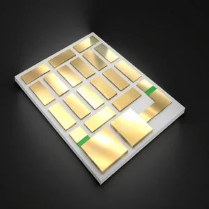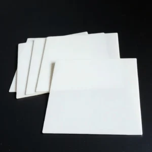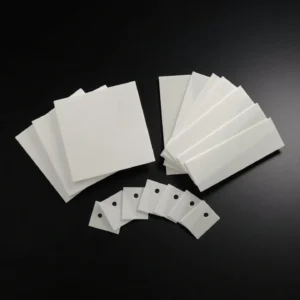
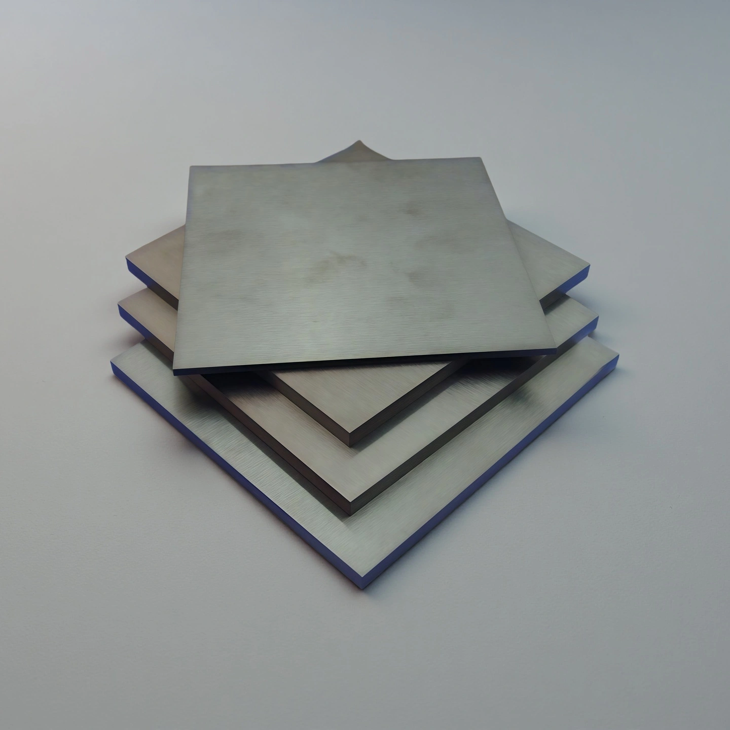
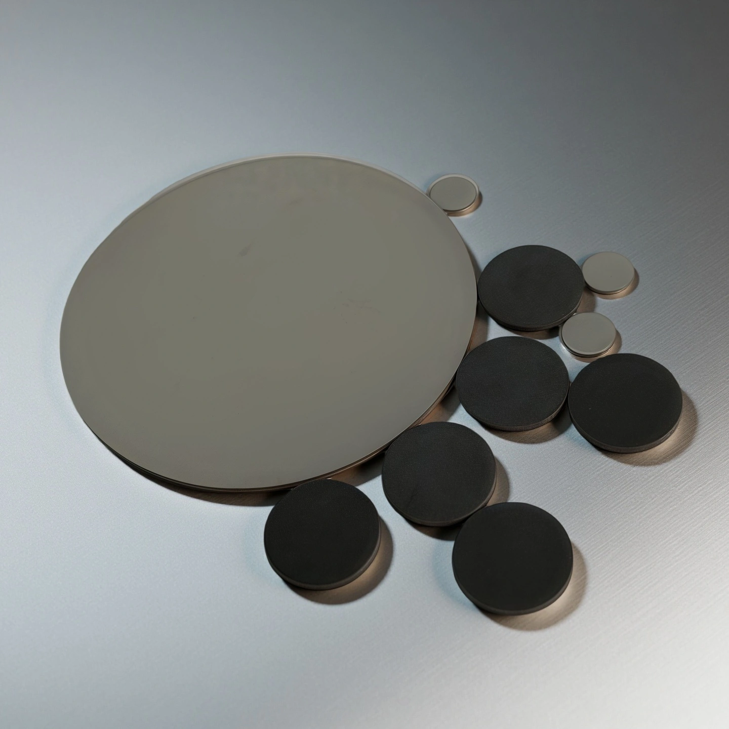
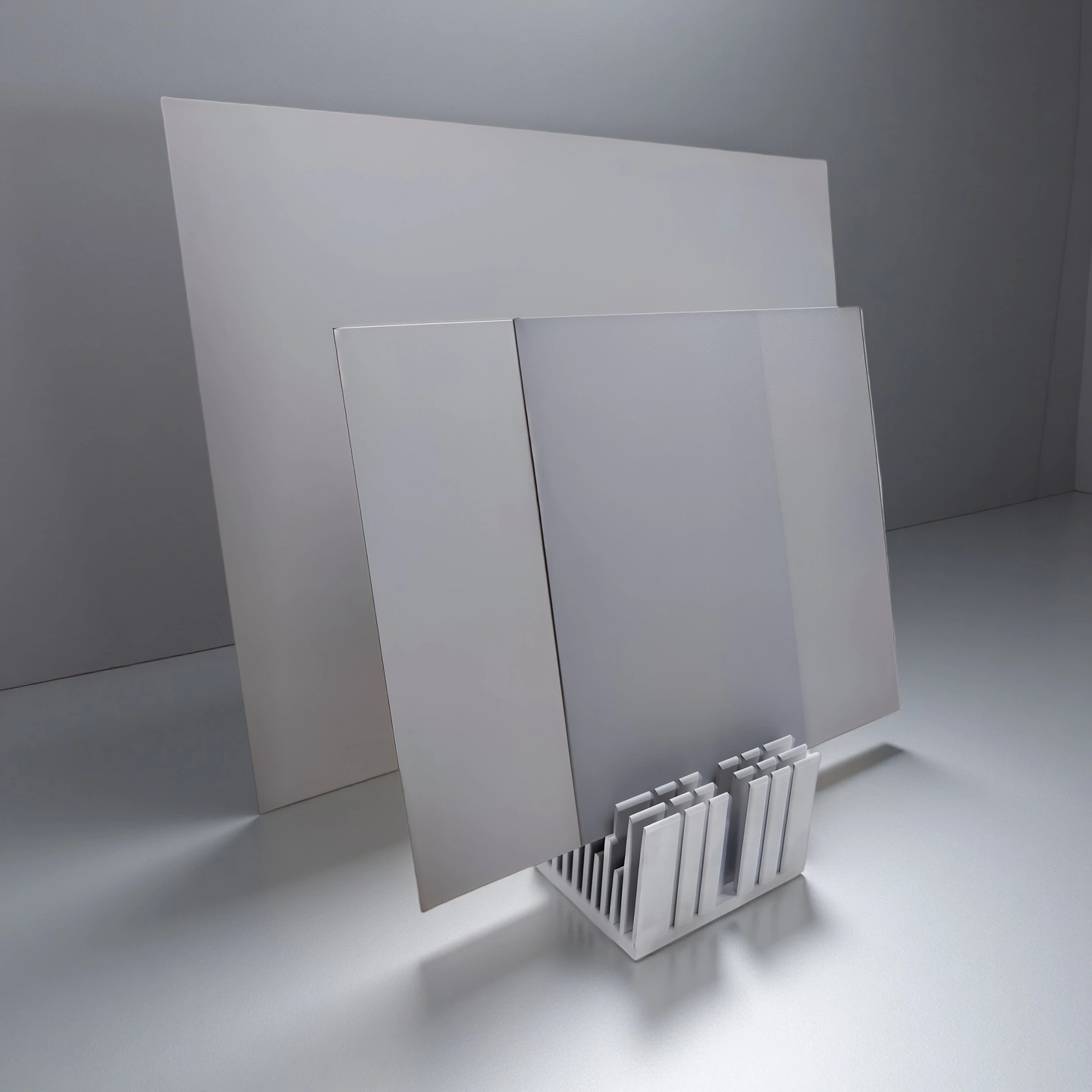
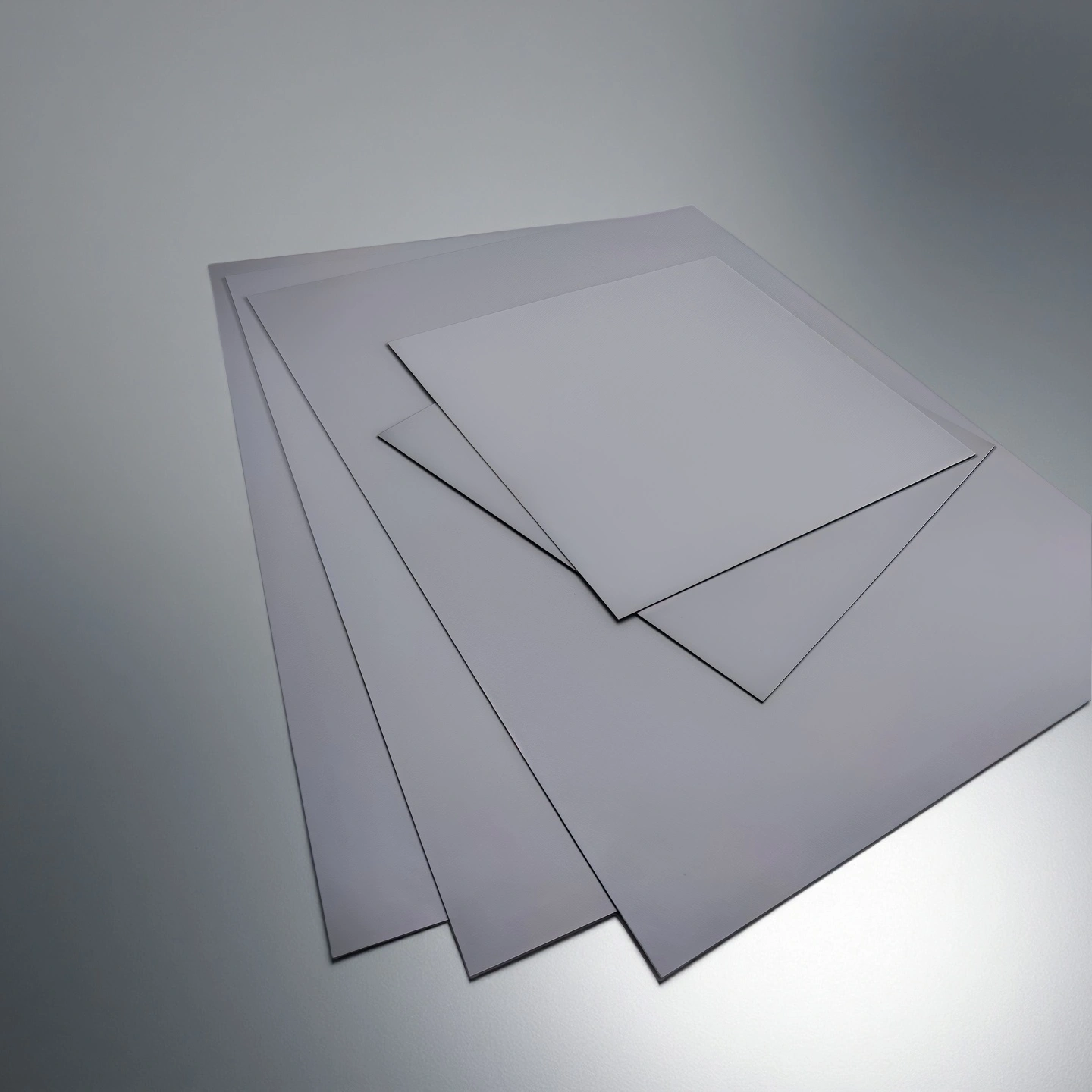
A high-strength silicon nitride substrate is an electrically insulating ceramic base used under copper metallization in SiC and IGBT power modules. It is selected when the module needs better thermal-cycling reliability, lower crack risk and stronger mechanical support than conventional alumina or aluminum nitride substrates.
Why Choose Si₃N₄ for Power Module Substrates?
Silicon nitride is selected when a power module substrate must balance thermal transfer, electrical insulation and mechanical reliability. Compared with alumina, Si₃N₄ provides higher thermal conductivity and fracture toughness. Compared with aluminum nitride, it is often selected where thermal cycling, vibration, copper stress and edge cracking are major reliability concerns.
| Material | Main Advantage | Limitation | Best-Fit Use |
|---|---|---|---|
| Alumina | Cost-effective and widely available | Lower thermal conductivity and lower toughness | Standard power circuits and cost-sensitive insulation |
| Aluminum Nitride | Very high thermal conductivity | More brittle under mechanical or thermal stress | Heat-spreading designs with controlled stress |
| Silicon Nitride | High toughness, good thermal conductivity and low CTE | Higher cost than alumina | SiC/IGBT modules, EV inverters and thermal-cycling assemblies |
High Strength Silicon Nitride Substrate Benefits
- High bending strength resists cracking under reflow and thermal cycling
Flexural strength above 600 MPa helps reduce substrate cracking risk during soldering and −40 °C to 150 °C cycling. This reduces die attach failures and supports long-term reliability evaluation in power modules. - 75–90 W/m·K thermal conductivity enables compact and cooler module design
Efficient heat transfer lowers junction-to-case resistance and supports high power density layouts. It supports more stable thermal paths in SiC and IGBT devices. - Dielectric strength ≥15 kV/mm supports thinner insulation and high-voltage safety
High insulation capability allows reduced substrate thickness without compromising creepage and clearance. Suitable for 800V EV systems, PV inverters, and industrial drives. - Low CTE close to SiC minimizes thermal stress on copper and die interfaces
With 2.9–3.2 × 10⁻⁶/K, the CTE matches semiconductor and metallization layers. This reduces solder fatigue, delamination, and warpage under rapid heating and cooling. - Precise flatness and thickness tolerance enhance metallization and solder bonding
Tight control of thickness (±0.05–0.10 mm) helps improve copper wetting consistency and brazing quality. It stabilizes thermal performance and helps reduce assembly variation when process conditions are controlled.
High Strength Silicon Nitride Substrate Properties
| Si3N4 Type | Gas pressure sintering Si3N4 | Hot pressing sintering Si3N4 | High thermal conductivity Si3N4 |
| Density (g/cm3) | 3.2 | 3.3 | 3.25 |
| Flexural Strength (MPa) | 700 | 900 | 600~800 |
| Young Modulus (GPa) | 300 | 300 | 300~320 |
| Poisson's ratio | 0.25 | 0.28 | 0.25 |
| Compressive strength (MPa) | 2500 | 3000 | 2500 |
| Hardness (GPa) | 15 | 16 | 15 |
| Fracture toughness (MPa*m1/2) | 5~7 | 6~8 | 6~7 |
| Maximum working temperature (℃) | 1100 | 1300 | 1100 |
| Thermal conductivity (W/m*K) | 20 | 25 | 80~100 |
| Thermal expansion coefficient (/℃) | 3*10-6 | 3.1*10-6 | 3*10-6 |
| Thermal shock resistance (ΔT ℃) | 550 | 800 | / |
High Strength Silicon Nitride Substrate Specifications
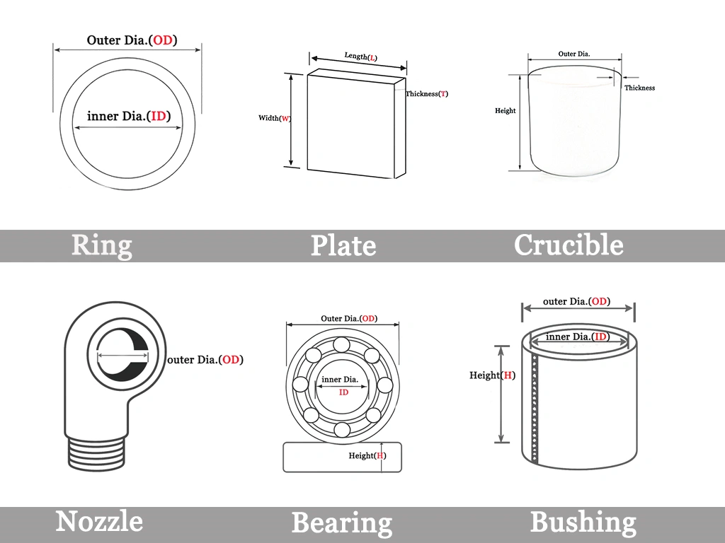
Type 1: Rectangular High Strength Silicon Nitride Substrate
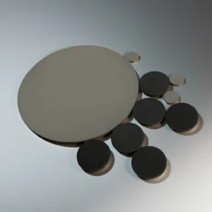
| Rectangular Silicon Nitride Substrate | |||
| Item No. | Length(mm) | Width (mm) | Thickness (mm) |
| AT-DHG-JB001 | 10 | 10 | 0.32 |
| AT-DHG-JB002 | 20 | 20 | 0.32 |
| AT-DHG-JB003 | 30 | 30 | 4.0 |
| AT-DHG-JB004 | 40 | 40 | 0.5 |
| AT-DHG-JB005 | 50 | 50 | 0.32 |
| AT-DHG-JB006 | 50 | 50 | 0.635 |
| AT-DHG-JB007 | 50 | 50 | 1.0 |
| AT-DHG-JB008 | 50 | 50 | 2.0 |
| AT-DHG-JB009 | 50 | 50 | 4.0 |
| AT-DHG-JB010 | 50 | 50 | 9.0 |
| AT-DHG-JB011 | 100 | 100 | 0.32 |
| AT-DHG-JB012 | 100 | 100 | 0.5 |
| AT-DHG-JB013 | 100 | 100 | 0.635 |
| AT-DHG-JB014 | 100 | 100 | 1.0 |
| AT-DHG-JB015 | 100 | 100 | 4.0 |
| AT-DHG-JB016 | 100 | 100 | 9.0 |
| AT-DHG-JB017 | 114 | 114 | 0.32 |
| AT-DHG-JB018 | 114 | 114 | 0.5 |
| AT-DHG-JB019 | 114 | 114 | 0.635 |
| AT-DHG-JB020 | 114 | 114 | 1.0 |
| AT-DHG-JB021 | 190 | 138 | 0.32 |
| AT-DHG-JB022 | 190 | 138 | 0.5 |
| AT-DHG-JB023 | 190 | 138 | 0.635 |
| AT-DHG-JB024 | 190 | 138 | 1.0 |
Type 2: Round High Strength Silicon Nitride Substrate
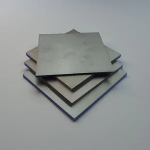
| Round Silicon Nitride Substrate | ||
| Item No. | Diameter(mm) | Thickness (mm) |
| AT-DHG-JB025 | 5 | 0.25 |
| AT-DHG-JB026 | 5 | 0.32 |
| AT-DHG-JB027 | 5 | 0.625 |
| AT-DHG-JB028 | 5 | 1 |
| AT-DHG-JB029 | 10 | 0.25 |
| AT-DHG-JB030 | 10 | 0.32 |
| AT-DHG-JB031 | 10 | 0.625 |
| AT-DHG-JB032 | 10 | 1 |
| AT-DHG-JB033 | 20 | 0.25 |
| AT-DHG-JB034 | 20 | 0.32 |
| AT-DHG-JB035 | 20 | 0.625 |
| AT-DHG-JB036 | 20 | 1 |
| AT-DHG-JB037 | 40 | 0.25 |
| AT-DHG-JB038 | 40 | 0.32 |
| AT-DHG-JB039 | 40 | 0.625 |
| AT-DHG-JB040 | 40 | 1 |
| AT-DHG-JB041 | 50 | 0.25 |
| AT-DHG-JB042 | 50 | 0.32 |
| AT-DHG-JB043 | 50 | 0.625 |
| AT-DHG-JB044 | 50 | 1 |
| AT-DHG-JB045 | 100 | 0.32 |
| AT-DHG-JB046 | 100 | 1 |
| AT-DHG-JB047 | 100 | 2 |
| AT-DHG-JB048 | 150 | 0.32 |
| AT-DHG-JB049 | 150 | 1 |
| AT-DHG-JB050 | 150 | 2 |
| AT-DHG-JB051 | 150 | 20 |
AMB/DBC Design Review Checklist
Before quotation, ADCERAX reviews the substrate drawing, copper layout and assembly conditions to reduce warpage, cracking and bonding risk. The following details help our team evaluate whether a standard substrate, custom blank or metallized substrate preparation is more suitable.
| Specification | What to Provide | Why It Matters |
|---|---|---|
| Substrate size | Length, width, diameter or panel outline | Confirms forming, cutting and inspection feasibility |
| Thickness | Ceramic thickness and tolerance | Affects insulation, thermal resistance and warpage |
| Copper layout | Copper thickness, symmetry and isolation gap | Reduces stress concentration and bonding risk |
| Flatness target | Bow or warpage limit after processing | Supports soldering, brazing and module assembly |
| Edge requirement | Chamfer, radius, bevel or deburring | Reduces edge chipping during handling |
| Surface finish | Bare, lapped, polished, Ni/Au, Ag or copper-ready | Supports solder wetting, wire bonding or metallization |
| Hole/slot features | Position, diameter, tolerance and datum | Helps avoid stress concentration and alignment errors |
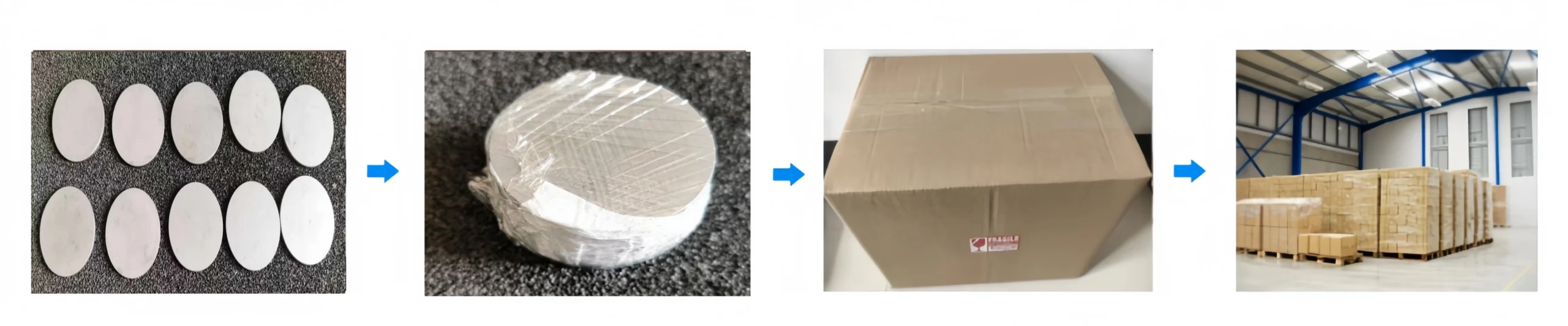
High Strength Silicon Nitride Substrate Packaging
- Each substrate is sealed in anti-static film
- Packed in foam-lined hard cartons to prevent breakage