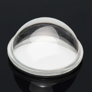
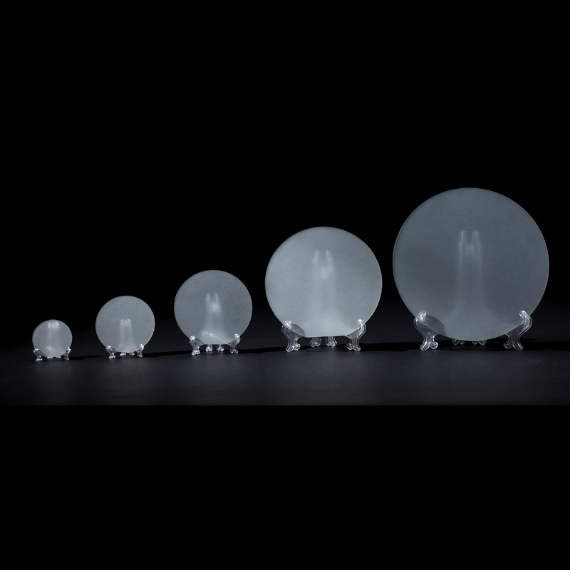
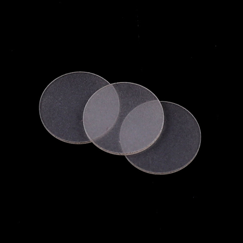
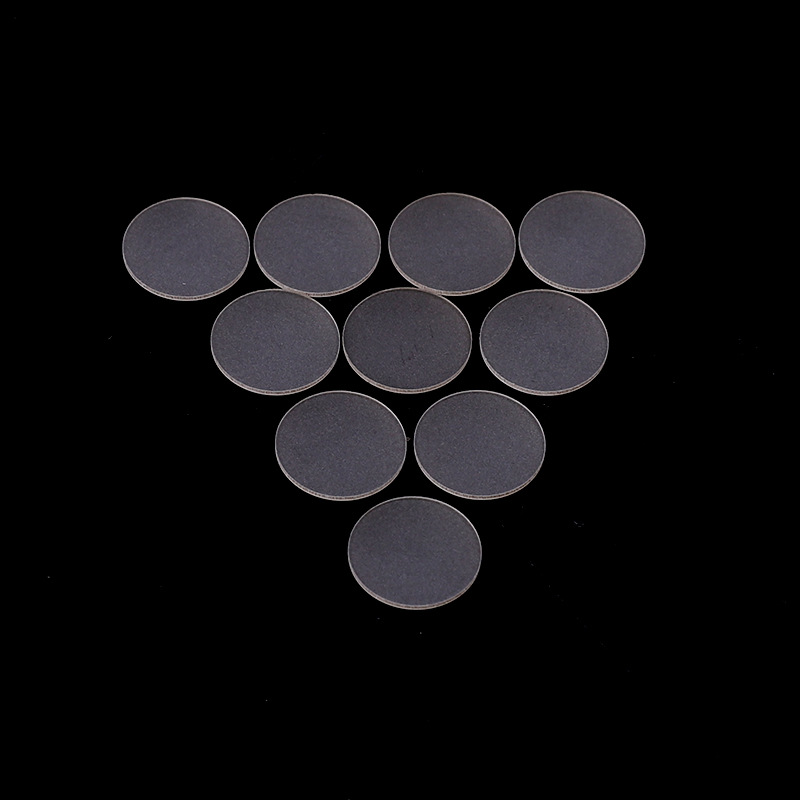
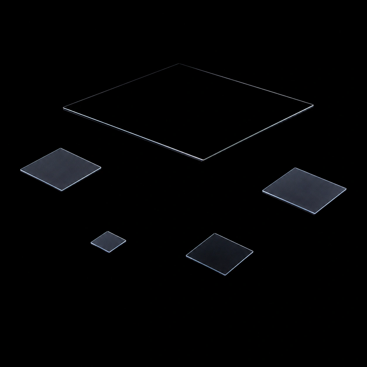
A sapphire substrate is a single-crystal Al₂O₃ wafer used as a base material for growing compound semiconductors like GaN and AlN. It provides high thermal conductivity, chemical stability, and optical transparency, making it essential for LED, LD, and optical coating applications.
Choose Your Sapphire Wafer Type
Standard C-Plane Sapphire Wafers
Common circular wafer formats for GaN/AlN epitaxy, LED and related thin-film processes. Configure diameter, thickness, SSP/DSP or epi-ready surface, flat/notch and geometry requirements.
Custom-Orientation Sapphire Wafers
A-, M- and R-plane wafers, with off-cut/miscut and specified orientation reviewed for SOS/RF, special epitaxy and R&D requirements. Additional orientations are project-reviewed.
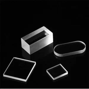
Square & Rectangular Sapphire Wafers
Cut-to-size sapphire substrates for research, thin-film deposition, device processing and fixture-specific layouts, with SSP/DSP/epi-ready surface options by specification.
Sapphire Wafer Selection Matrix
| Application | Recommended Wafer Direction | Key Specifications to Define |
|---|---|---|
| GaN/AlN epitaxy and LED manufacturing | C-plane (0001), epi-ready | Diameter, off-cut, SSP or DSP, roughness measurement method, TTV, Bow, Warp, flat or notch configuration, and cleanliness requirements. |
| SOS, RF, and microelectronics | R-plane is commonly evaluated, while the final orientation depends on the device process. | Crystal orientation, miscut or off-cut, thickness, surface finish, and electrical or process requirements. |
| Special, non-polar, or semi-polar applications | A-plane, M-plane, or another specified orientation is reviewed according to the project. | Exact Miller index, orientation tolerance, off-cut direction and angle, and polished-side requirements. |
| Thin-film or experimental substrates | C-plane, A-plane, M-plane, R-plane, or a project-specific orientation. | Shape, dimensions, thickness, surface finish, wafer geometry, and cleaning requirements. |
| Non-circular fixtures or coupons | Square or rectangular cut-to-size sapphire substrates. | Length, width, thickness, crystal orientation, polished side, edge or chamfer design, TTV, and flatness. |
Common Sapphire Wafer Configurations
| Product Family | Common Format | Orientation | Surface Options | Geometry and Custom Fields | Status |
|---|---|---|---|---|---|
| Standard circular wafers | Common 1-, 2-, 3-, 4-, 5-, 6-, and 8-inch formats. | C-plane (0001). | SSP, DSP, or epi-ready. | Thickness, flat or notch configuration, off-cut, and grade-specific TTV, Bow, and Warp requirements. | These formats are within the common sourcing range. The final specifications must be confirmed for each RFQ. |
| Custom-orientation wafers | Standard or custom diameters. | A-plane, M-plane, R-plane, or another specified orientation subject to review. | As-cut, ground, SSP, DSP, or epi-ready, as applicable. | Orientation tolerance, off-cut angle and direction, flat or notch configuration, and thickness. | A-plane, M-plane, and R-plane are core options. Additional crystal planes require project-specific review. |
| Square or rectangular wafers | Cut to the specified dimensions. | C-plane, A-plane, M-plane, R-plane, or a project-specific orientation. | SSP, DSP, or epi-polished. | Length, width, thickness, edge configuration, polished side, TTV, flatness, and packaging. | This is a custom substrate format and should not be described as a sapphire window. |
| Patterned sapphire substrates | Project-specific formats. | The orientation is determined by the application. | Patterned and epi-ready surfaces according to the application requirements. | Pattern geometry, dimensions, surface condition, and epitaxy requirements. | This should only be presented as a related option, subject to project review. |
Sapphire Substrate Specifications
Type 1: Sapphire Substrate Round
| Sapphire Substrate Round | ||
| Item NO. | Diameter (mm) | Thickness (mm) |
| AT-BS-JP1001 | 5 | 0.3 |
| AT-BS-JP1002 | 9 | 1 |
| AT-BS-JP1003 | 25.4 | 0.6 |
| AT-BS-JP1004 | 50 | 0.3 |
| AT-BS-JP1005 | 50 | 0.4 |
| AT-BS-JP1006 | 100 | 0.65 |
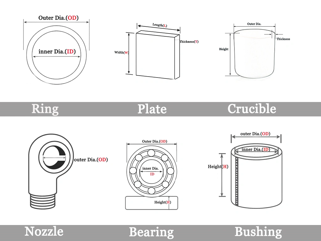
| AT-BS-JP1007 | 1-80 customize | 0.09-10 customize |
Type 2: Sapphire Substrate Square
| Sapphire Substrate Square | ||
| Item NO. | Length (mm) | Thickness (mm) |
| AT-BS-JP1008 | 21*5 | 0.6 |
| AT-BS-JP1009 | 30*18 | 0.4 |
| AT-BS-JP1010 | 60*55 | 0.4 |
| AT-BS-JP1011 | 60*55 | 0.6 |
| AT-BS-JP1012 | 60*55 | 0.8 |
| AT-BS-JP1013 | 60*55 | 1.14 |
| AT-BS-JP1014 | (1.9-60)*(1.0-55) customize | 0.09-10 customize |
Sapphire Substrate Properties
| Property | Typical / Reference Value |
|---|---|
| Material | Single-crystal Al₂O₃, also known as synthetic sapphire. |
| Density | Approximately 3.97–3.98 g/cm³. |
| Crystal Structure and Lattice Parameters | Corundum single crystal with lattice parameters of approximately a = 4.758 Å and c = 12.991 Å. |
| Thermal Conductivity | Approximately 23–46 W/(m·K) at room temperature. The actual value depends on crystal orientation and the test method. |
| Coefficient of Thermal Expansion | Approximately 4.3–7.7 × 10⁻⁶/K. The actual value depends on crystal orientation and temperature. |
| Volume Resistivity | Greater than 10¹⁴ Ω·cm at room temperature as a typical reference value. |
| Hardness | Mohs hardness of 9. |
Sapphire Substrate Route, Inspection & Packaging
Typical wafer production route:
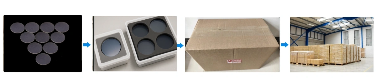
Single-crystal material/boule selection → crystal orientation verification → slicing or dicing → lapping/grinding → SSP, DSP or CMP / epi-ready polishing → controlled cleaning → dimensional & surface inspection → protective packaging. The exact route and acceptance criteria are defined by the approved wafer specification.
| Inspection Point | What Is Checked | RFQ / Document Link |
|---|---|---|
| Crystal Orientation | Crystal plane or Miller index, off-cut direction, and off-cut angle. | Orientation requirements. |
| Dimensions | Diameter or length × width, thickness, flat or notch configuration, and edge geometry. | Drawing or wafer specification. |
| Wafer Geometry | TTV, Bow, Warp, and flatness. | Specified acceptance limits. |
| Surface | SSP, DSP, or epi-ready finish, surface roughness, measurement method, and visual surface condition. | Surface grade and test method. |
| Cleanliness | Clean handling, packaging method, and visible contamination criteria. | Process and packaging specifications. |
| Identification | Lot number, label, and marking requirements. | Traceability requirements. |
| Packaging | Protective separation, wafer box, cassette, or individual packaging. | Order quantity and shipping requirements. |