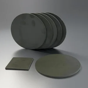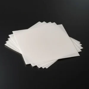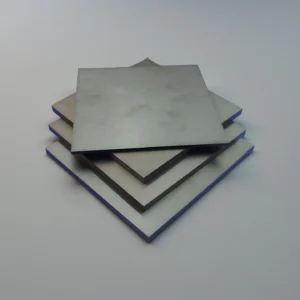
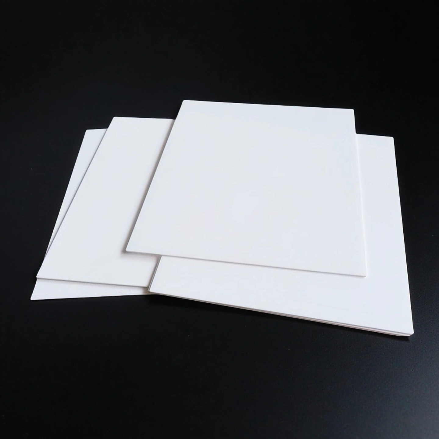
Custom ZTA Ceramic Substrates for Heaters, Sensors & LED Modules

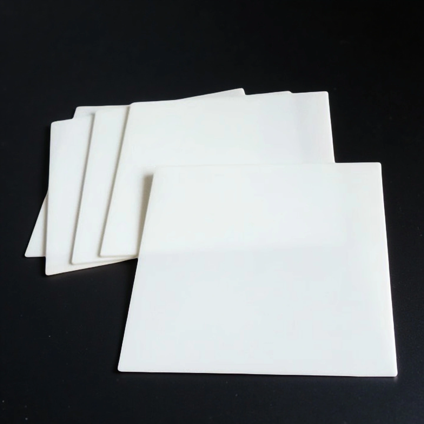
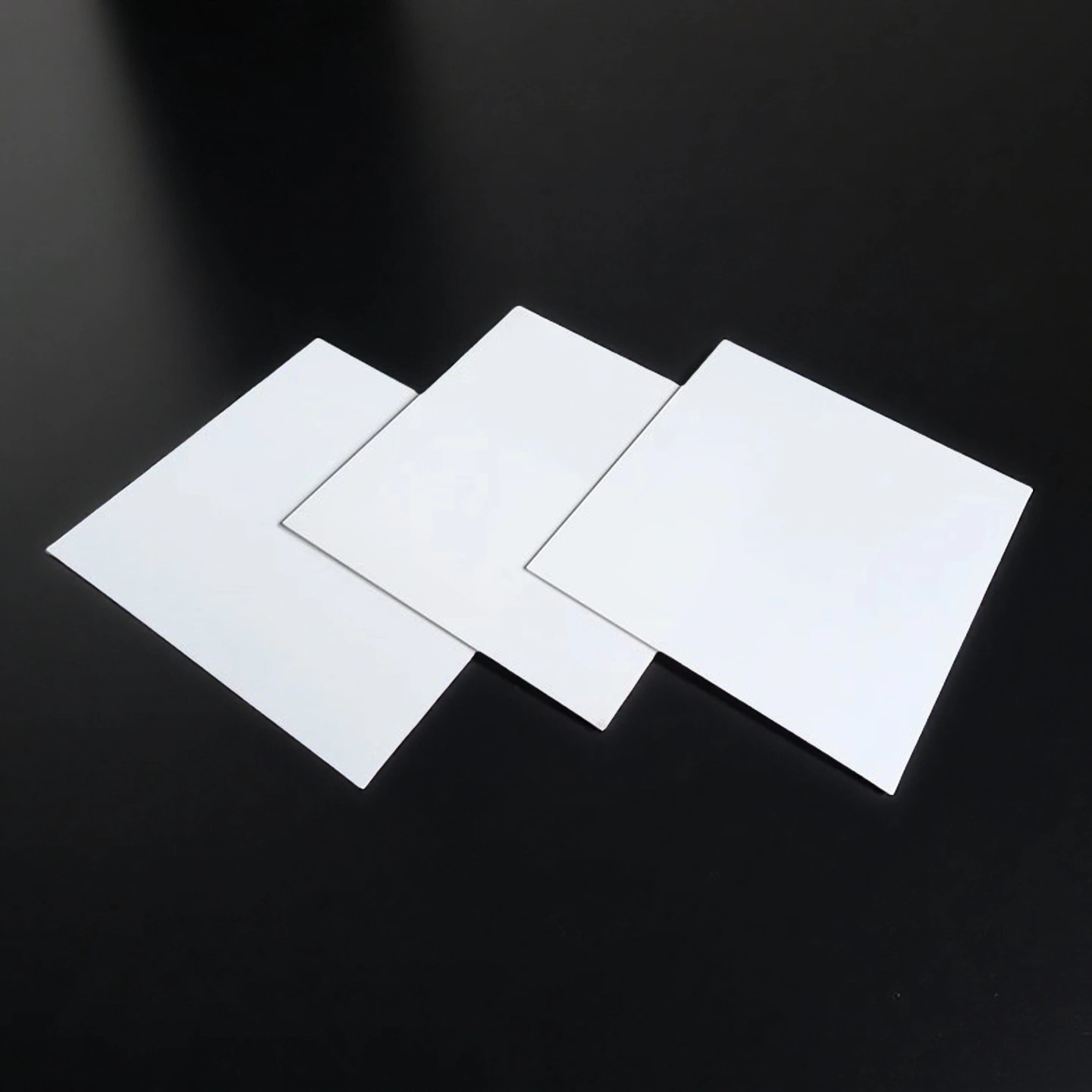
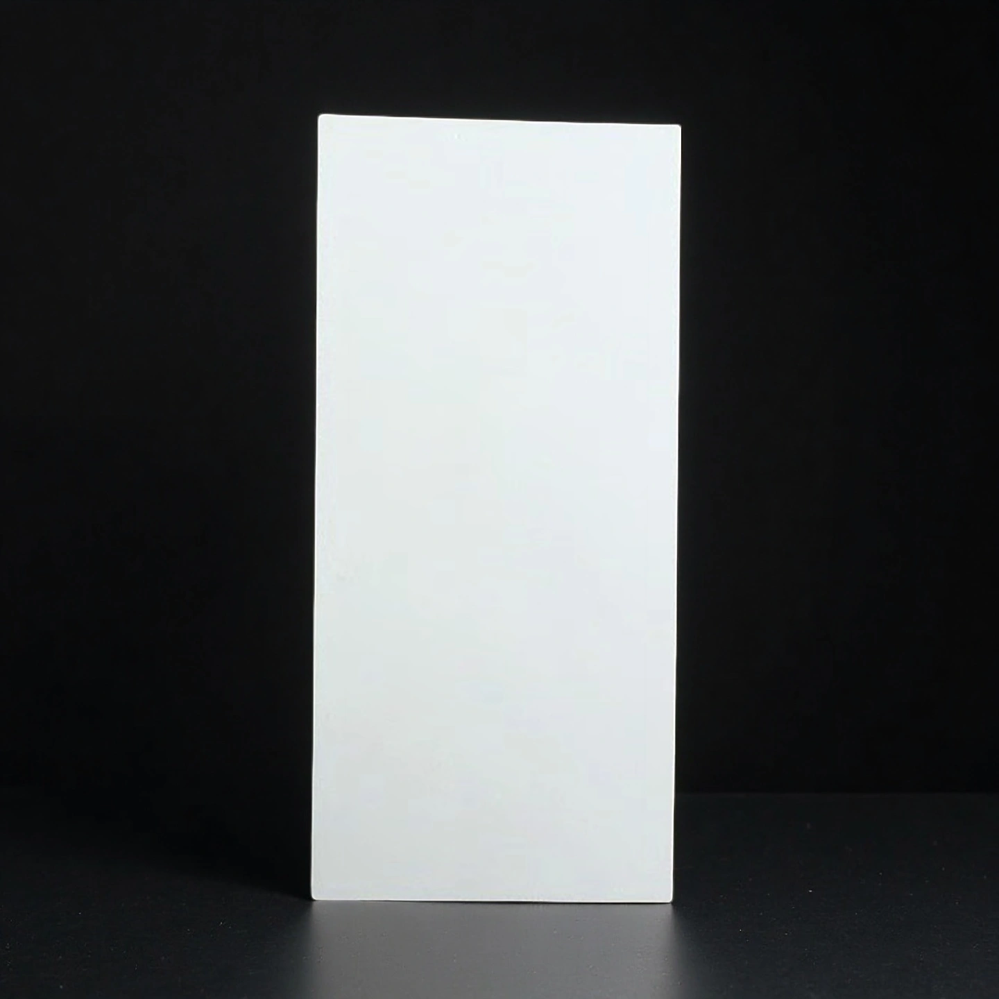
ADCERAX supplies custom ZTA ceramic substrates for thick-film heaters, sensors, LED/UV modules and precision insulating carriers. ZTA provides better edge toughness and chip resistance than standard alumina around laser-drilled holes, slots and scribed outlines while maintaining insulation and dimensional stability.

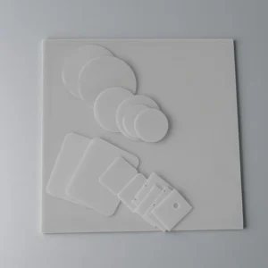
Standard blanks and custom sizes are available with laser vias, slots, chamfers, lapped surfaces, Ra control and metallization-ready preparation.

Catalogue No. AT-ZTA-CS001
Typical Composition ZrO₂-toughened Al₂O₃ ceramic
Main Use Heaters, sensors, LED/UV modules, control boards
Custom Features Laser vias, slots, scribed outlines, chamfers
Surface Options As-fired, ground, lapped or polished
Engineering RFQ Review
Small-Batch Custom Support
Factory-Direct Manufacturing
Drawing & Process Review

What Are ZTA Ceramic Substrates?

ZTA ceramic substrates are insulating ceramic base plates made by adding zirconia particles into an alumina matrix. The alumina phase provides electrical insulation, chemical stability and dimensional control, while the zirconia phase improves fracture toughness and helps reduce edge chipping around holes, slots and scribed outlines.

For engineers working with thick-film circuits, heater patterns, sensor carriers or LED/UV modules, ZTA is often selected when standard alumina is easy to chip during laser drilling, handling or assembly, but full zirconia is not required.

Why Use ZTA Instead of Standard Alumina?

Buyer Concern Standard Alumina ZTA Ceramic Substrate Selection Meaning
Edge chipping around holes Moderate risk on thin or micro-featured parts. Better edge toughness and crack resistance. Better for vias, slots and scribed outlines.
Electrical insulation Strong. Strong. Both can work for insulating carriers.
Surface preparation Mature and cost-effective. Suitable for ground, lapped and print-ready surfaces. ZTA is useful when print quality and edge integrity both matter.
Thermal conductivity Usually higher than zirconia. Similar to high-grade alumina in many substrate uses. Suitable for medium-power modules, not a replacement for AlN in high heat-spreading designs.
Cost Usually lower. Higher than standard alumina. Use ZTA when chipping, strength or yield loss justifies the upgrade.

ZTA Substrates Advantages

  • Edge integrity on micro-features — reduced chipping on laser-drilled vias/slots.
  • Print-ready surface — controlled Ra and flatness for screen printing and bonding.
  • Dimensional stability — consistent thickness and geometry across batches.
  • White/reflective option — uniform appearance for optical/LED modules.
  • Traceable cleanliness — cleaned, bagged, labeled for immediate line use.

ZTA Ceramic Substrate Properties

Property Unit Alumina (99%) ZTA (Zirconia Toughened Alumina) Y-TZP Zirconia
Fracture Toughness (KIC) MPa·m¹⁄² 5 7 – 9 6 – 10
Hardness (HV10) GPa 8.9 9 – 10 (≈ 90 HV) 12 – 14
Flexural Strength MPa 400 650 – 800 800 – 1200
Density g/cm³ 3.9 4.0 – 4.3 6.0
Relative Wear Rate 1.0 0.45 – 0.55 0.2
Thermal Expansion Coefficient (RT – 800 °C) ×10⁻⁶ /K 8.0 8.5 – 9.0 10 – 11
Thermal Conductivity (RT) W/m·K 25 22 – 24 2 – 3
Maximum Working Temperature °C 1600 1450 – 1500 1000 – 1200
Dielectric Strength kV/mm 12 11 – 13 9 – 11
Surface Roughness (Ground face) µm Ra 0.4 – 1.2 0.3 – 0.8 0.2 – 0.6
Flatness (after grinding) mm/300 mm ≤ 0.4 ≤ 0.3 ≤ 0.2


Specifications of Zirconia Toughened Alumina Substrates

Item Length(mm) Width(mm) Thickness(mm) Purity (Al₂O₃+ZrO₂)
AT-ZTA-CS001 10 10 0.5 74%+23.5%
AT-ZTA-CS002 10 10 1 74%+23.5%
AT-ZTA-CS003 15 11 1.5 74%+23.5%
AT-ZTA-CS004 18 13 1.5 74%+23.5%
AT-ZTA-CS005 20 20 2 74%+23.5%
AT-ZTA-CS006 20 20 2 74%+23.5%
AT-ZTA-CS007 25 25 1 74%+23.5%
AT-ZTA-CS008 30 30 0.5 74%+23.5%
AT-ZTA-CS009 30 30 1 74%+23.5%
AT-ZTA-CS010 30 30 2 74%+23.5%
AT-ZTA-CS011 35 35 1 74%+23.5%
AT-ZTA-CS012 40 40 1 74%+23.5%
AT-ZTA-CS013 40 40 3 74%+23.5%
AT-ZTA-CS014 50 30 0.5 74%+23.5%
AT-ZTA-CS015 50 50 0.5 74%+23.5%
AT-ZTA-CS016 50 50 1 74%+23.5%
AT-ZTA-CS017 50 50 1.5 74%+23.5%
AT-ZTA-CS018 50 50 2 74%+23.5%
AT-ZTA-CS019 60 60 1 74%+23.5%
AT-ZTA-CS020 65 35 0.5 74%+23.5%
AT-ZTA-CS021 65 48 1 74%+23.5%
AT-ZTA-CS022 70 70 1.2 74%+23.5%
AT-ZTA-CS023 70 70 3 74%+23.5%
AT-ZTA-CS024 76.2 76.2 1.5 74%+23.5%
AT-ZTA-CS025 80 80 3 74%+23.5%
AT-ZTA-CS026 80 80 2 74%+23.5%
AT-ZTA-CS027 80 70 1.5 74%+23.5%
AT-ZTA-CS028 84 84 0.8 74%+23.5%
AT-ZTA-CS029 100 100 0.5 74%+23.5%
AT-ZTA-CS030 100 100 1 74%+23.5%
AT-ZTA-CS031 100 100 1.2 74%+23.5%
AT-ZTA-CS032 100 100 1.5 74%+23.5%
AT-ZTA-CS033 100 100 2 74%+23.5%
AT-ZTA-CS034 100 90 1.5 74%+23.5%
AT-ZTA-CS035 100 80 1.8 74%+23.5%
AT-ZTA-CS036 100 75 2 74%+23.5%
AT-ZTA-CS037 10-400 10-400 0.5-2.5 74%+23.5%


Design and RFQ Guidelines for ZTA Substrates

To quote ZTA ceramic substrates accurately, please provide a drawing or sample with the required outline, thickness, hole diameter, slot width, tolerance, flatness or warp requirement, surface roughness target, quantity and downstream process.

For printed heater or sensor substrates, please also indicate whether the surface will be used for thick-film printing, bonding, soldering, DPC preparation, metallization or optical alignment. This helps ADCERAX review the correct surface finish, cleaning method, inspection plan and packaging method before production.

ZTA Ceramic Substrate Packaging

  • All ceramic substrates are individually wrapped in anti-static, padded sheets, sealed, and placed in custom-cut foam-lined boxes to ensure maximum protection.
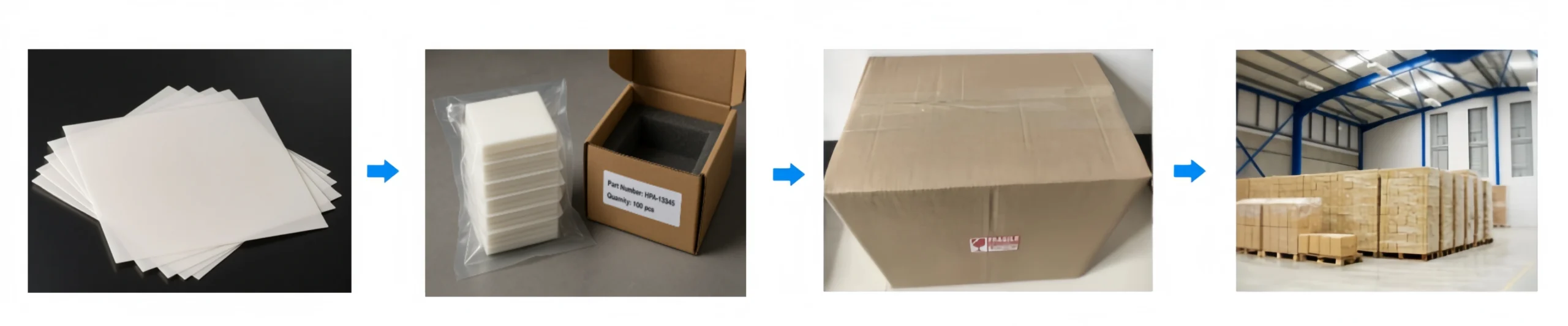
ZTA Ceramic Substrate Packaging


Applications of Zirconia Toughened Alumina Substrates

Application Buyer Problem Why ZTA Helps Common Custom Requirements
Thick-Film Heaters Standard alumina may chip around holes or scribed edges during printing, firing or assembly. ZTA improves edge toughness while keeping an insulating ceramic surface for resistor patterns. Lapped surface, Ra control, laser scribing, via holes, low warp.
Sensor Carriers Sensor assemblies need stable geometry, clean surfaces and reliable bonding zones. ZTA supports thin insulating carriers with better mechanical robustness than standard alumina. Fiducials, slots, polished or lapped surfaces, serialized marking.
LED / UV Modules COB or UV modules require reflective, stable and clean ceramic support surfaces. White ZTA substrates can support optical alignment and reduce edge damage during assembly. Controlled whiteness, flatness, surface gloss, clean packaging.
Control Electronics Ceramic carriers may need slots, locator holes and insulation stability. ZTA balances machinability, insulation and mechanical toughness for small-format circuit carriers. Laser vias, countersinks, chamfers, dimensional inspection.
Pilot Production and Custom Modules Early-stage programs need small batches before tooling or design freeze. ZTA blanks can be customized by drawing for pilot validation and DFM review. Small-batch production, drawing review, tolerance stack check.

Usage Instructions of ZTA Substrates

  • Install

    1. Verify flatness/warp vs. fixture plan; shim only within specified range.
    2. Align fiducials before printing/placement; confirm vacuum chuck contact on lapped side.
    3. Use edge-safe grippers; avoid point loads at micro-holes or slot ends.

  • Use

    1. Match Ra and paste type; run a short DOE for print speed/snap-off and bake profile.
    2. For laser operations, validate pulse energy and pitch on sacrificial pieces first.
    3. If metallizing, control pre-clean, bake-out, and cure windows per paste and surface.

  • Store

    1. Keep in original clean bags; control humidity and dust.
    2. Stack with interleaves; avoid cantilevered storage that induces warp over time.

  • Clean

    1. Non-ionic detergent or solvent compatible with downstream paste/adhesive.
    2. DI water rinse and lint-free dry; avoid abrasive wipers on polished surfaces.

  • Cautions

    1. Do not exceed specified clamp force on thin sections.
    2. Avoid thermal shock beyond validated ramp/soak profiles.
    3. Re-inspect Ra/flatness if re-lapping or rework occurs.

  • Typical user pitfalls & fixes

    1. Issue: Print voids near slots → Fix: Reduce snap-off, adjust squeegee hardness, confirm local Ra.
    2. Issue: Lens misalignment on large panels → Fix: Tighten warp limit, use full-contact vacuum chuck.
    3. Issue: Edge chips at micro-holes → Fix: Add micro-chamfer, tune laser parameters, update handling jaws.

Zirconia Toughened Alumina Ceramic Substrate

  1. Q: Can ZTA substrates be laser drilled or laser scribed?
    A: Yes. ZTA substrates can be laser drilled, slotted, scribed or trimmed according to drawings. Minimum hole size, edge quality and positional tolerance should be confirmed through DFM review, especially for thin substrates or dense micro-hole patterns.
  2. Q: What surface finish is available for ZTA ceramic substrates?
    A: ADCERAX can provide as-fired, ground, lapped or polished ZTA substrate surfaces. For thick-film printing, bonding or optical assembly, customers should specify the required Ra value, flatness, active surface side and any cleaning or packaging requirements.
  3. Q: Can ZTA ceramic substrates be used for thick-film printing?
    A: Yes. ZTA substrates can be prepared for thick-film heater patterns, sensor circuits and printed conductive or resistive layers. The final print quality depends on surface roughness, flatness, paste system, firing profile and pattern design.
  4. Q: Can ZTA substrates be metallized or plated?
    A: ZTA substrates can be prepared for metallization, plating or bonding processes after surface review. Please provide the target metallization system, bonding method, operating temperature and inspection requirement so the surface finish and cleaning process can be matched.
  5. Q: What thickness and size can be customized?
    A: ZTA substrate thickness, outline, holes, slots, chamfers and surface finish can be customized according to drawings. Standard sizes may be available, while larger or thinner parts should be reviewed based on flatness, warp, handling risk and production yield.
  6. Q: What information is needed for a quotation?
    A: Please provide a drawing or sample with length, width, thickness, tolerance, hole or slot data, flatness or warp requirement, surface roughness target, quantity, application and downstream process. If the part will be printed, bonded, metallized or optically aligned, include those details in the RFQ.
  7. Q: How are ZTA ceramic substrates packed?
    A: ZTA substrates are typically cleaned, separated with protective interleaves, packed in padded or foam-lined boxes and labeled by batch. For optical, printing or bonding applications, clean packaging and handling instructions can be discussed before production.
customize size

Customize Ceramic ZTA Substrates

Provide your drawing or target window and select from the options below; our engineers will review DFM, tolerance stack, and inspection plan. What you can specify:

1. Outline & Size
• Max outline: up to 200 × 200 mm
• Thickness range: 0.25 – 2.0 mm
• Custom shapes: rectangular, circular, or irregular per drawing

2. Tolerances
• Thickness / linear: ±0.05 – ±0.10 mm
• Edge chamfer: C- or R-type, adjustable width
• Hole/slot position: laser aligned, repeatability ±0.05 mm

3. Features
• Options: through-vias, blind holes, slots, countersinks
• Locator steps and fiducials for precision alignment
• Laser-engraved ID marks or QR codes for tracking

4. Surface Options
• Finishes: as-fired / ground / lapped/polished
• Roughness: target Ra ≤ 0.8 µm, single or both sides
• Optical use: controlled whiteness and gloss uniformity

5. Laser Processes
• Operations: scribing, micro-drilling, edge trimming
• Quality: burr-free control on slots and micro-holes
• Optional serialization or marking for batch traceability

6. Metallization Readiness
• Compatible with Ag/Pd, Pt, Au paste systems
• Optional Ni/Au plating after joint process approval
• Surface energy controlled for bonding and solder adhesion

Related Products

ADCERAX - Your Trusted Advanced Ceramics Manufacturing Partner

Direct factory manufacturing with comprehensive ceramic materials expertise and global supply capabilities

China-Based Manufacturer

ADCERAX supplies ceramic components for overseas OEMs, equipment builders, and labs.

Custom Drawing Support

We review drawings, dimensions, materials, and application conditions before quotation.

Ceramic Process Control

Forming, sintering, machining, grinding, and finishing are arranged by part requirements.

Pre-Shipment Inspection

Dimensional checks, visual inspection, and packaging review help reduce procurement risk.

Get in Touch with Us

Our team will be happy to respond to you in less than 24 hours.

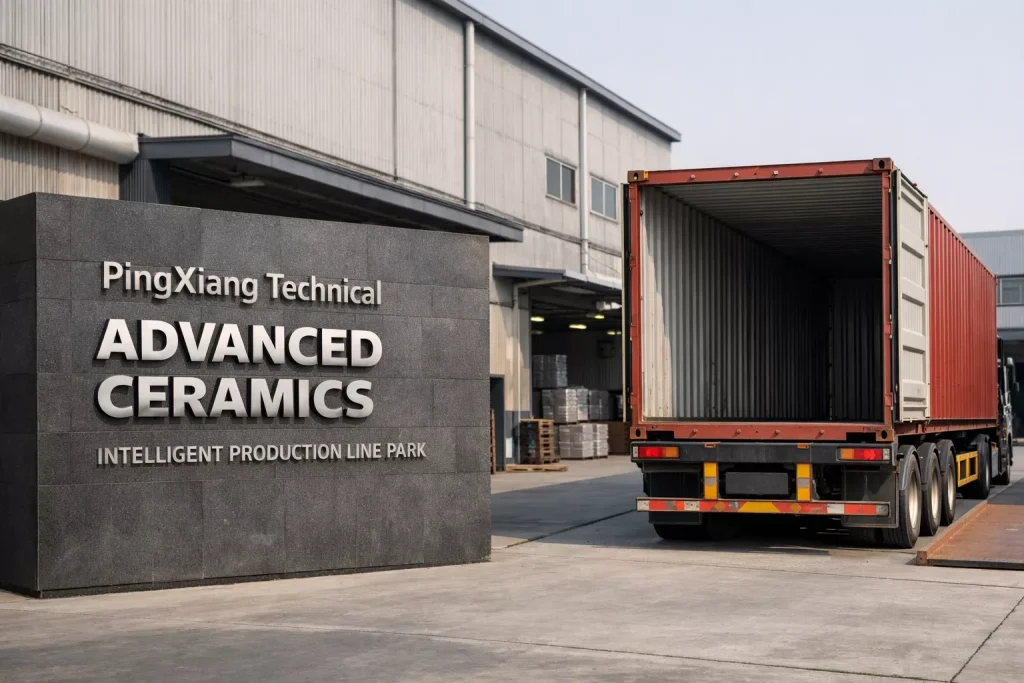
Pingxiang Factory — Silicon carbide, silicon nitride, high-temperature ceramics

Quick Quotation

*Our team will answer your inquiries within 24 hours.

*Your information will be kept strictly confidential.

Ready to Solve Your Engineering Challenge?

Partner with ADCERAX for reliable, high-performance advanced ceramic solutions. Our engineers are ready to discuss your project.

E-mail

info@adcerax.com

Phone

+(86) 0731-74427743 | WhatsApp: +(86) 19311583352

Response Time

Within 24 hours

Quick Quote

The more details you provide, the faster we can quote.

*We respond within 24 hours. All inquiries are confidential.

Get Your Custom Solution

The more details you provide, the faster we can respond.

customize size

*We respond within 24 hours. All inquiries are confidential.

Download Catalog