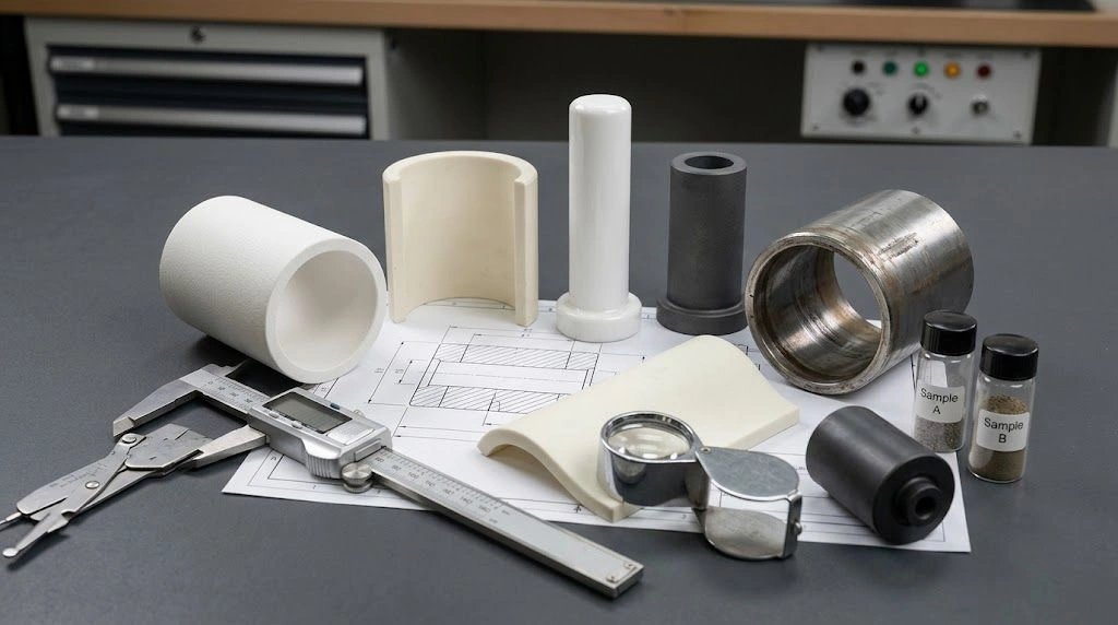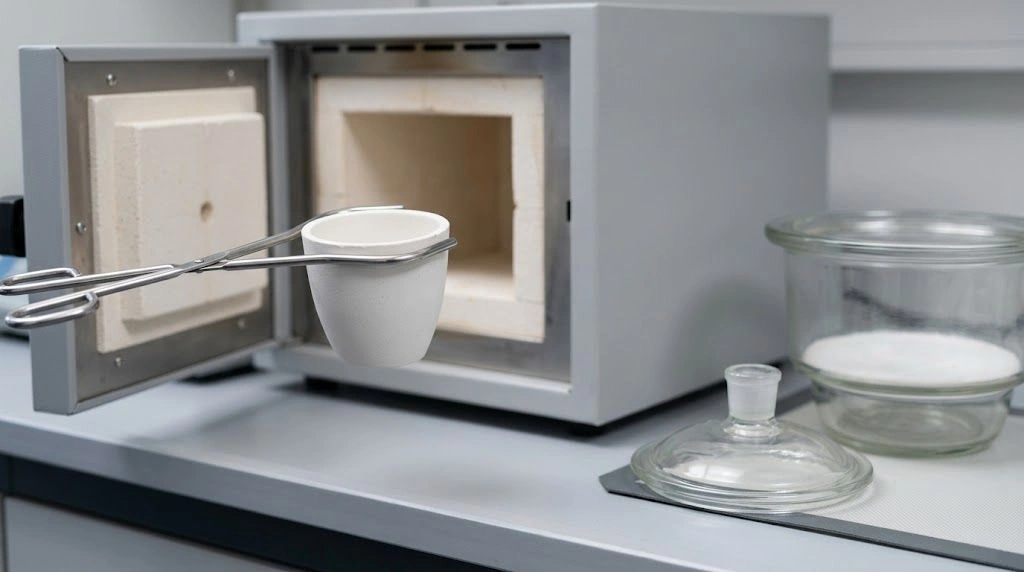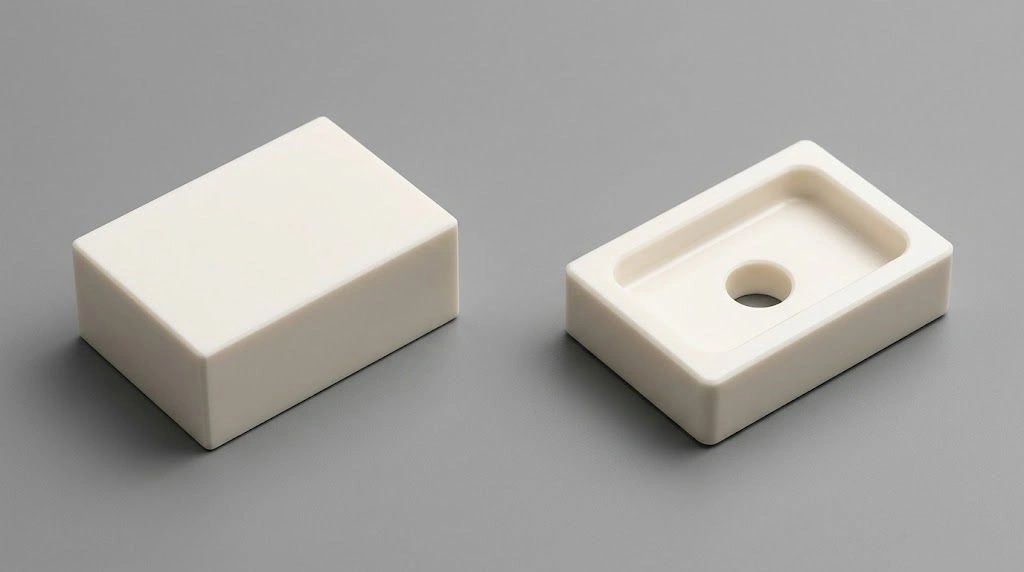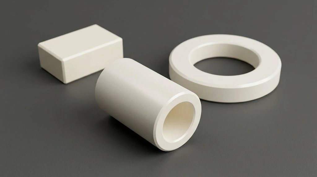
BN crucibles can support silicon ingot growth only when purity, melt interaction, temperature window, and crucible geometry are matched to the growth method. Hot-pressed BN may help with non-wetting release and machinable custom shapes, while PBN is preferred when higher purity, dense walls, and low outgassing are required. For molten silicon, shape cannot be separated from purity: wall thickness, bottom radius, taper, fill height, and rim design affect thermal field, sticking, stress, and ingot release — and a high-purity crucible with wrong geometry will fail at the same problem as a lower-purity crucible with right geometry.
The engineering discipline this guide imposes is to treat purity and shape as co-equal specification variables, not as independent choices where purity is the material decision and shape is just the drawing detail.
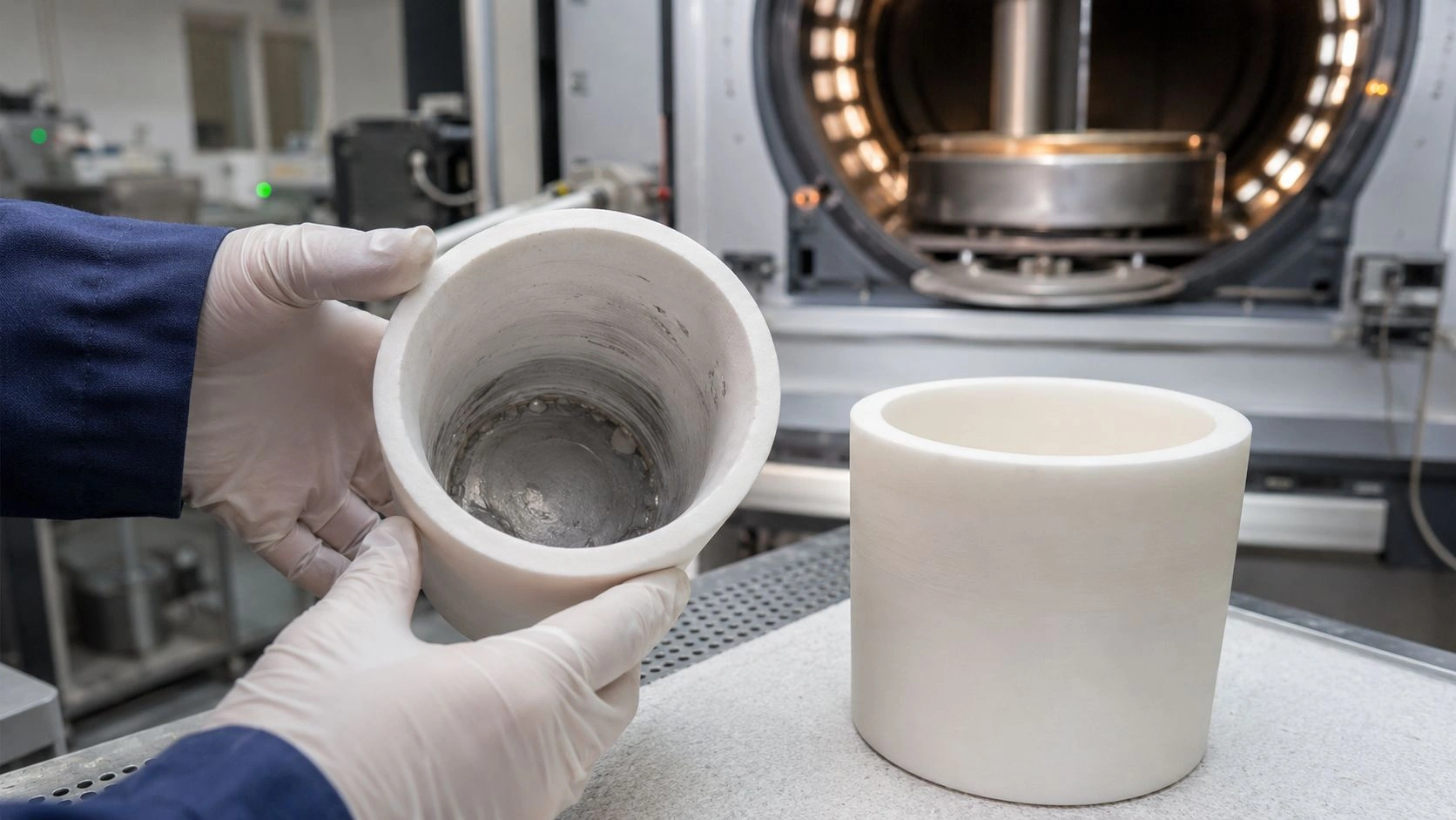
BN and PBN crucibles in silicon ingot growth must be evaluated for both purity — to control melt contamination — and shape — to manage heat transfer, sticking, and ingot release.
The boron nitride crucibles for high-purity melting and crystal growth applications at ADCERAX include hot-pressed BN for machinable custom geometries and PBN for dense-wall, low-outgassing, semiconductor-adjacent applications — both available with custom cavities, tapered bores, flanged rims, and drawing-based dimensional specifications.
When BN or PBN crucibles make sense for silicon ingot growth
BN and PBN crucibles should be evaluated for silicon ingot growth when the process requires clean melt containment, reduced sticking, custom crucible geometry, or a non-carbon ceramic interface. The route must be validated against molten silicon behavior and the specific growth method — it is not automatically superior to conventional quartz or Si₃N₄-coated systems.
In silicon crystal growth practice, silicon is melted in crucibles at temperatures above approximately 1400°C. Published silicon melting and crystallization reviews frame crucible selection around thermal properties, contamination, wetting behavior, reusability, and design together — not around material name alone. That framing is exactly right for BN: the material's non-wetting behavior, chemical compatibility, and machinable geometry are advantages only when the specific temperature window, melt contact conditions, and process geometry support them.
The practical boundary is this: BN and PBN are most appropriate for R&D, specialty silicon, controlled crystallization experiments, and growth configurations where silicon contact is intermittent or where conventional quartz and coating options impose constraints the BN route resolves. They are not automatically a production-scale replacement for established silicon ingot practice.
BN/PBN as a conditional silicon melt-contact route
"Conditional" means the route requires validation before commitment. The wetting behavior of molten silicon on BN changes with temperature, the purity sensitivity of silicon depends on the target application, and the geometry of a BN crucible influences whether release, stress, and thermal-field requirements can be met. None of those can be assumed from the material specification sheet alone.
Why standard silicon ingot crucible practice still matters
Conventional silicon ingot production uses quartz crucibles with Si₃N₄-based release coatings in many directional solidification and casting configurations. Those routes have well-characterized contamination profiles, established process windows, and supply chains. Published research specifically evaluates Si₃N₄ coatings as interface releasing agents for photovoltaic silicon ingot growth — confirming that the established practice involves deliberate interface design, not the crucible material alone.
Where lab-scale and specialty growth differ from mass production
For laboratory-scale crystallization, comparative material experiments, small-batch specialty silicon, or growth configurations where an engineered BN interface is the research variable, BN and PBN offer geometry flexibility and a defined chemical interface that conventional quartz does not provide. For mass production, the validation effort, cost, and supply-chain readiness of BN routes must be evaluated against those requirements — a different question from material performance.
Purity route: hot-pressed BN or PBN?
For silicon ingot growth, purity selection should start with the contamination pathway — which impurities matter, at what level, and which material route minimizes them.
Hot-pressed BN is attractive for silicon melt-contact applications when custom geometry, machinability, and non-wetting release behavior are the primary requirements. It can be machined to complex cavity shapes, tapers, flanges, and stepped bases that conventional powder-pressed or molded ceramics cannot achieve in a single piece.
PBN becomes the stronger candidate when the application requires dense gas-tight walls, low outgassing in vacuum or controlled atmosphere, and a purity level consistent with semiconductor-adjacent cleanliness. Published ADCERAX PBN crucible documentation positions CVD-formed PBN with typical purity above 99.99%, dense wall structure, and custom cavity profiles as appropriate for crystal growth including silicon when semiconductor-grade purity and gas-tight containment are required.
The BN/PBN Decision Matrix below maps the six key selection variables:
| Decision variable | Hot-pressed BN may fit when | PBN may fit when | Verify before RFQ |
|---|---|---|---|
| Purity requirement | Custom geometry and non-wetting behavior are primary | High-purity, dense wall, and low outgassing are primary | COA, impurity basis, cleaning method |
| Melt-contact risk | Lab-scale or specialty trial accepts validation testing | Semiconductor-adjacent cleanliness is required | Small silicon melt-contact trial |
| Shape complexity | Machined cavities, taper, flanges, stepped bases needed | CVD wall profile can meet geometry need | Drawing feasibility |
| Wall density | Some porosity / machined BN route acceptable | Gas-tight wall required | Wall structure and leak/outgassing expectation |
| Release behavior | Taper and radius can manage demolding | Smooth dense wall needed for cleaner release | Wetting/sticking test |
| Size / cost boundary | Larger or complex shapes needed | Smaller high-purity vessels acceptable | Size capability and lead time |
Values indicative; verify with supplier-specific BN/PBN grade data, silicon melt-contact testing, and application trials.
However, purity does not replace melt-contact testing. Published Si/h-BN wetting research reports that increasing temperature improves wetting and that a non-wetting-to-wetting transition occurs around 1650°C under studied argon conditions — which is within the temperature range used in silicon melting. That means a BN surface that provides non-wetting release in one temperature window can behave differently in another. [CITE: Published Springer research on Si/h-BN wetting behavior reports a non-wetting-to-wetting transition at approximately 1650°C under argon conditions, confirming that temperature-dependent wetting must be validated for the specific silicon melt-contact conditions rather than assumed from low-temperature BN non-wetting data or material purity specifications alone.]
Hot-pressed BN: machinability and custom geometry
The primary manufacturing advantage of hot-pressed BN in silicon ingot applications is that it can be machined to drawing-specified custom geometries — taper angles, bottom radii, stepped bases, overflow ports, and flanged rims — that cannot be readily produced in PBN by CVD growth. For research-scale crystallization experiments where the crucible geometry is itself a variable, that machining flexibility is directly useful.
PBN: dense wall, low outgassing, and high-purity route
PBN's advantages come from its CVD formation process: the wall is dense, gas-tight, and free of the sintering aids, binders, or grain-boundary phases that can contribute impurities in hot-pressed ceramics. For silicon applications where oxygen, metallic, or other ceramic-derived impurities at trace levels are a process concern, PBN provides a more controlled contamination baseline — at the cost of higher unit price and more constrained geometry customization at larger scales.
Shape variables that affect silicon melt behavior and ingot release
Crucible shape affects silicon ingot growth because it changes how heat transfers from the external heating system through the ceramic wall to the melt, how the solidifying silicon interacts with the crucible surface during cooling, and whether the ingot can be removed without damage after solidification.
The Shape Variables table below maps seven geometry parameters to their engineering consequences:
| Shape variable | Why it matters | Poor-spec risk | RFQ wording |
|---|---|---|---|
| Wall thickness | Controls heat transfer and strength margin | Thermal lag or fragile wall | "Confirm wall thickness and tolerance" |
| Bottom radius | Reduces corner stress and material locking | Sticking, cracking, difficult release | "Specify internal bottom radius" |
| Inner taper | Supports ingot release after shrinkage | Straight-wall sticking | "Confirm inner taper angle" |
| H/D ratio | Affects melt depth and thermal zone fit | Vertical thermal gradient mismatch | "Confirm capacity and fill height" |
| Rim / lip | Controls handling and atmosphere boundary | Chipping or contamination from tools | "Define lip, chamfer, and handling feature" |
| Lid / cover | May reduce vapor or particle exposure | Uncontrolled atmosphere or contamination | "Confirm lid clearance and seating" |
| Surface finish | Affects release and cleaning | Residue retention | "Confirm machined or polished surface condition" |
Published silicon crystallization reviews frame crucible design as a co-equal criterion alongside contamination, wetting, and thermal properties — confirming that geometry specification is not a secondary detail but a primary selection variable for silicon melt-contact applications.
The PBN crucibles for crystal growth and vacuum evaporation at ADCERAX support custom wall profiles, bore geometries, and cavity shapes that can be specified by drawing — but each geometric feature must be described by its engineering function (bottom radius for stress and release, taper for demolding, rim for handling) rather than as a catalog dimension.
Wall thickness and thermal gradient
In silicon ingot growth, crucible wall thickness determines how much thermal resistance sits between the external heat source and the silicon melt. Thicker walls increase thermal lag between the heating system and the melt inner surface, which affects both melt temperature uniformity and the effective temperature at the silicon-ceramic interface. For thin-wall PBN configurations, the thermal resistance is lower but the mechanical margin is smaller — requiring careful attention to fill level and handling.
Bottom radius and solidification stress
Molten silicon that solidifies against a sharp internal corner experiences concentrated stress during cooling contraction. A rounded inner bottom radius distributes that stress and reduces the risk of the solidifying ingot locking into the corner — one of the documented causes of ingot damage during extraction. The radius should be specified on the drawing with a minimum value, not left to shop practice.
Taper angle and ingot release
Silicon contracts as it solidifies and cools. A straight-wall crucible cavity creates a shrink-fit condition as the ingot cools against the ceramic. A slight inward taper on the cavity wall creates a geometry where the ingot's shrinkage allows it to move away from the wall during cooling rather than gripping it. The appropriate taper angle depends on the silicon ingot geometry, expected shrinkage, and fill height, and should be part of the drawing specification.
Do not misdiagnose purity problems when wetting or shape is the cause
The Misdiagnosis Matrix below maps five common silicon ingot failure symptoms to their correct diagnostic questions:
| Observed problem | Common assumption | Better diagnostic question |
|---|---|---|
| Silicon sticks to BN | BN purity is too low | Did temperature enter a wetting transition window, and is taper sufficient? |
| Ingot release causes damage | Material route is wrong | Are bottom radius, wall taper, and cooling shrinkage compatible? |
| Contamination appears | Crucible is the only source | Did feedstock, atmosphere, graphite hardware, handling, or coating contribute? |
| Thermal nonuniformity | Crucible material is wrong | Does shape fit the thermal field and furnace geometry? |
| PBN trial fails | PBN purity is insufficient | Was the wall profile, fill height, and melt-contact condition validated? |
Diagnostic questions are starting points; confirm with post-run crucible inspection, ingot analysis, and process history.
Published Si/h-BN wetting research documents that wetting behavior changes with temperature — confirming that sticking at elevated silicon melting conditions may reflect a temperature-driven wetting change rather than a material purity failure. A BN or PBN crucible that appears to perform well at lower temperatures or in short exposure may behave differently under sustained high-temperature contact, and that distinction must be part of the failure diagnosis before a material change is specified.
The safest engineering rule for silicon ingot BN crucible selection: do not diagnose "purity is wrong" until wetting temperature, taper angle, bottom radius, and cooling rate have been evaluated as independent variables. Each of those can cause sticking and release damage independently of the ceramic purity level.
Coating or liner interface failures
When a BN liner is used inside a graphite or quartz outer body, the liner-to-body interface can introduce its own failure modes — uneven contact creating local hot and cold spots, or materials from the outer body migrating to the melt through gaps or cracks. These are system-level failures, not BN material failures, and they require fixture-and-assembly diagnosis rather than material-upgrade diagnosis.
The ceramic crucible options at ADCERAX — spanning BN, PBN, alumina, zirconia, and SiC — provide cross-material context when evaluating whether a full BN crucible, a BN liner inside graphite, or a different ceramic material entirely is the appropriate route for the specific silicon growth configuration.
RFQ checklist for BN/PBN crucibles in silicon ingot growth
Before submitting an RFQ for a BN or PBN crucible for silicon ingot growth, resolve the growth method, purity target, shape variables, and validation plan together — not sequentially.
The minimum RFQ data package:
- Growth method — Czochralski, Bridgman, directional solidification, float zone, or custom configuration; this determines the thermal profile, crucible mechanical loading, and release conditions.
- Silicon grade — electronic grade, solar grade, experimental purity, or specialty specification; this determines how sensitive the application is to boron, nitrogen, oxygen, or metallic contamination from the ceramic.
- Melt temperature range — minimum, working, and peak temperature; specifically relevant because of the wetting transition behavior documented in Si/h-BN research.
- Atmosphere and pressure — argon, nitrogen, vacuum, or controlled atmosphere; atmosphere affects both BN oxidation boundary and silicon-ceramic interfacial reaction.
- Target ingot geometry — diameter, height, and mass; these determine the crucible ID, fill height, and whether the taper angle needs to accommodate the specific ingot shrinkage geometry.
- Crucible drawing — OD, ID, height, wall thickness, bottom thickness, bottom radius, inner taper, rim/lip design, lid requirement, flange, surface finish, and dimensional tolerance.
- Validation plan — specify whether a small silicon melt-contact trial is required before batch supply; this is especially important when the temperature window approaches or may exceed the documented wetting transition.
- Supplier verification data — request BN or PBN grade confirmation, purity basis and COA, wall density or outgassing expectation, machining tolerance class, cleaning and packing method, and maximum recommended operating temperature by atmosphere.
[CITE: Expert engineering guidance on BN/PBN crucible selection for silicon ingot growth confirms that a conditional, test-based, drawing-driven approach — specifying purity route, shape geometry, temperature validation, and melt-contact trial together before batch commitment — is the correct engineering framework, because neither purity alone nor geometry alone determines whether the crucible performs in silicon melt-contact service.]
Evaluating BN or PBN crucibles for silicon ingot growth? Share your growth method, silicon grade, melt temperature range, atmosphere, target ingot geometry, fill height, and crucible drawing. ADCERAX engineers return a purity-route recommendation with shape guidance, dimensional feasibility, and validation trial options for the confirmed growth configuration; turnaround depends on inquiry complexity — no RFQ commitment required at this stage.
Frequently Asked Questions
Can BN crucibles be used for silicon ingot growth?
Yes, after validating molten silicon interaction, temperature window, purity requirement, and crucible geometry for the specific growth method. BN and PBN should be treated as a conditional route that requires application-specific testing rather than a universal replacement for quartz or Si₃N₄-coated conventional crucibles.
Is PBN better than hot-pressed BN for silicon ingot growth?
PBN is preferred when dense walls, low outgassing, and higher purity are the primary requirements. Hot-pressed BN may be more practical when machinability, large or complex custom shapes, and non-wetting release are the main design needs. The correct choice depends on whether contamination control or geometry customization is the binding constraint for the specific growth configuration.
Does molten silicon wet boron nitride?
Published Si/h-BN wetting research reports that wetting improves with increasing temperature and that a non-wetting-to-wetting transition occurs around 1650°C under studied argon conditions. This means silicon melt-contact testing at the actual process temperature is important before qualification, because low-temperature non-wetting data does not automatically predict behavior in the silicon melting range.
Why does crucible shape matter for silicon ingots?
Shape affects thermal gradients, melt depth, solidification stress distribution, sticking behavior, ingot demolding, and furnace fit. Wall thickness, bottom radius, taper angle, height-to-diameter ratio, rim design, and surface finish are all drawing-level specification variables — not secondary details to be resolved after material selection.
Should a silicon ingot BN crucible always have a taper?
A taper is often useful for release, but the correct angle depends on ingot geometry, silicon shrinkage behavior, fill height, and furnace design. It should be specified by drawing based on the release engineering of the specific configuration — not assumed from a catalog shape or copied from a different growth process.
What should be sent to a supplier for BN/PBN crucible evaluation?
Send the growth method, silicon grade, melt temperature range, atmosphere, target ingot diameter and height, fill height, crucible drawing with all geometric parameters (OD/ID/height/wall/bottom radius/taper/rim), purity target, and the planned validation test — specifically whether a silicon melt-contact trial is required before batch supply. The combination of process conditions, drawing, and validation plan allows the supplier to confirm purity route, geometry feasibility, and recommended testing sequence.