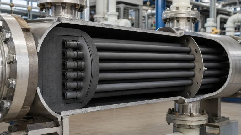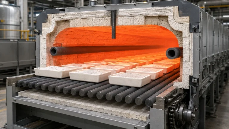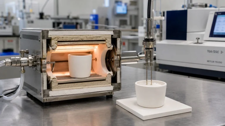
PBN components are used in ion implantation systems when source-zone or beamline hardware must combine high purity, low outgassing, electrical insulation, high-temperature stability, and low metal contamination risk. Typical roles include source insulators, extraction-electrode insulators, spacers, rings, shields, liners, tubes, and source-facing custom components. PBN is not selected simply because it can withstand high temperature — it is selected when contamination control, vacuum behavior, dopant-gas compatibility, plasma exposure, and particle control are more important than low material cost. The correct specification requires the exact component role, the dopant chemistry it will face, the thermal and electrical environment, and the contamination target — not just the material name.
The PBN crucibles and low-outgassing custom PBN components at ADCERAX — produced by CVD for MBE, vacuum evaporation, and high-purity semiconductor source applications — provide the material context for the ion implantation component decisions described in this guide.
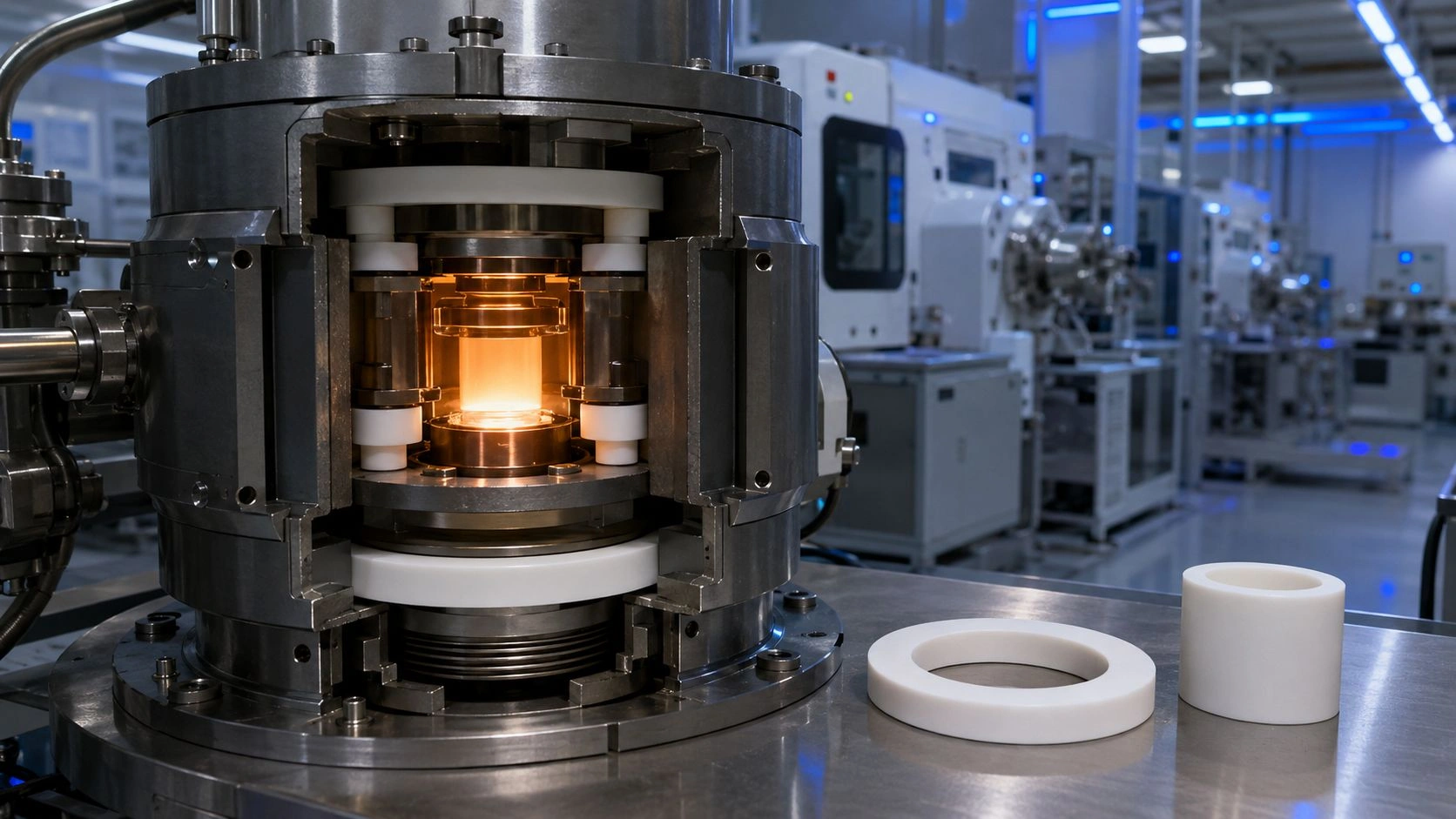
PBN components in ion implantation systems serve as source insulators, extraction-electrode insulators, spacers, rings, and source-facing liners — their value is contamination control and electrical insulation, not only high-temperature capability.
Where PBN components fit in ion implantation systems
Ion implantation systems cover a sequence of hardware zones from the ion source through extraction optics, mass analysis, acceleration/deceleration optics, and beamline to the wafer process chamber. The source area concentrates the most demanding conditions: dopant gases or vapors at elevated temperature, plasma, high electrical potential, and corrosive process chemistry fragments are all present simultaneously.
Published review of ion implantation technology confirms that ions are generated from a gas or solid source at the ion source arc block and extracted by the extraction electrode. This sequence creates the specific component positions where PBN and BN materials are considered — not across the entire implanter, but at the hardware closest to the source and extraction regions where electrical insulation, high temperature, corrosive gas compatibility, and contamination control intersect.
Historical ion implanter design patents confirm this material use: they describe high-temperature ceramic insulators including boron nitride used around ion-source hardware exposed to corrosive precursor gases such as BF₃ and SiF₄ and their reaction fragments. Published ion implanter extraction electrode insulation guidance confirms the requirement for materials combining high-temperature tolerance, resistance to strong electrical fields, resistance to aggressive process gases, and mechanical durability in the insulator zone.
The PBN Component Roles in Ion Implantation Systems table maps each hardware position:
| Component role | Function | Why PBN helps | Main risk | What to verify |
|---|---|---|---|---|
| Source insulator | Electrically isolates hot source hardware | High-purity insulation, low metal risk | Dopant corrosion, thermal stress | Dopant gas, temperature, voltage |
| Extraction electrode insulator | Supports high-field extraction region | Insulation near hot/corrosive source zone | Beam strike, deposits, arcing | Geometry, dielectric clearance |
| Spacer/ring | Maintains alignment and isolation | Low outgassing, clean support | Clamp cracking or particles | Mounting pressure, edge finish |
| Shield/liner | Separates source hardware from contamination path | Clean source-facing surface | Deposit flaking or sputtering | Plasma/beam exposure |
| Tube/sleeve | Insulates or separates heated source features | Thermal stability and insulation | Thermal gradient cracking | Wall thickness and fit |
| Custom source-facing part | Replaces metal or lower-purity ceramic in sensitive zone | Lower metal contamination pathway | Cost and geometry limit | Qualification data and FAI |

PBN component selection in ion implantation systems should start from hardware role — source insulators, extraction-electrode insulators, spacers, shields, tubes, sleeves, and custom source-facing parts each carry different contamination, insulation, dopant chemistry, and qualification risks.
Why PBN is considered: low metals, low outgassing, and electrical insulation
After mapping the hardware positions, the material argument for PBN over alternative insulators in those zones becomes more specific.
[CITE: A 2025 ICIS ion source process-integrity presentation confirms that modern semiconductor ion source requirements include low metal contamination as essential for advanced nodes and CMOS image sensors, alongside low wafer particles, long source lifetime, and uptime targets — and Axcelis technical documentation on low-metals ion source design confirms that low-level metallic contaminants represent device risks for CMOS image sensors including white pixels, dark current, carrier lifetime reduction, gate oxide breakdown, threshold voltage shifts, and junction leakage — establishing that PBN component specification for ion implantation is driven by device-yield contamination requirements, not only by source-zone temperature or chemical resistance in isolation.]
Low metal contamination for wafer yield. PBN is CVD-grown boron nitride without metallic binders, sintering aids, or free-metal phases. Its contamination contribution to the ion source environment is limited to boron and nitrogen — elements that are already implant species in many processes and that do not carry the device-degrading risks associated with metallic contaminants such as iron, copper, nickel, or chromium. In contrast, metal hardware in the source zone — arc chamber components, clamps, brackets, electrodes — can sputter or outgas metal atoms that reach the wafer. Substituting metal-facing hardware with PBN insulators in critical source positions can reduce this pathway.
Low outgassing for vacuum stability. PBN's CVD-grown dense structure — virtually no porosity, no residual solvents or organics, no binder phases — makes it one of the lower outgassing ceramic options for UHV-adjacent environments. Shin-Etsu describes PBN as combining heat resistance with electrical insulation in a high-purity structure produced from BCl₃ and NH₃ by chemical vapor deposition. Kennametal positions PBN as an ultra-high-purity BN grade grown by CVD and suited to high-temperature contamination-free applications.
Electrical insulation under high temperature and bias. The ion source zone operates at elevated temperature — often above 600–800°C for Freeman or Bernas-type sources — with electrical potentials applied for arc discharge and ion extraction. The insulating material must maintain dielectric performance under this combined thermal and electrical stress without cracking, creeping, or introducing conductive deposits. PBN retains good electrical insulation to high temperature while remaining chemically stable in the presence of fluorine-containing and hydride dopant gas chemistries.
Why PBN is not the same as hot-pressed BN. The manufacturing route matters for source-zone applications. Hot-pressed BN is a machinable and cost-effective insulating ceramic, but its powder-derived structure is more porous and may carry higher validation requirements for low-outgassing and particle-sensitive use. The boron nitride ceramic custom parts range at ADCERAX covers both hot-pressed BN tubes, rods, rings, plates, washers, and nozzles for general high-temperature insulation use, and PBN components for the most demanding contamination-critical positions.
PBN vs hot-pressed BN, alumina, quartz, and graphite
After establishing why PBN is considered, the comparison with alternative insulator materials helps identify where PBN's advantage is material and where other options remain adequate.
The PBN vs Other Materials for Ion Implanter Components table maps the main options:
| Material route | Best-fit use | Main advantage | Main boundary |
|---|---|---|---|
| PBN | Source-facing clean insulators, rings, shields, liners | High purity, low outgassing, electrical insulation | Cost, thin-wall geometry limits |
| Hot-pressed BN | Machinable high-temp insulators away from most critical zones | Easy machining and thermal shock resistance | Porosity/outgassing validation burden |
| Alumina | General ceramic insulators and supports | Cost-effective dielectric ceramic | Particle and purity validation needed |
| Quartz | Clean insulating parts in selected zones | Low contamination in many semiconductor tools | Thermal/erosion limits |
| Graphite | Hot conductive source hardware | Thermal stability and machinability | Conductive; carbon/particle risk |
| Refractory metals | Electrodes, arc chamber, structural hot parts | Conductive and mechanically robust | Metal contamination/sputtering risk |
PBN vs alumina. Alumina is widely used in semiconductor equipment as a cost-effective dielectric ceramic. Its particle and purity performance depends critically on grade, surface finish, and cleaning procedure. In source-facing positions where direct plasma exposure or dopant chemistry contact is possible, alumina may require more validation to confirm its particle and contamination contribution is within specification. PBN's CVD structure reduces this validation burden for the most sensitive positions.
PBN vs quartz. Quartz is clean in many semiconductor tool contexts and provides good dielectric performance. Its limitation in ion source applications is thermal behavior at repeated cycling and potential for sputter erosion if directly exposed to the ion beam. PBN handles higher temperature with better thermal shock resistance and retains cleanliness in aggressive fluorine chemistry.
PBN vs graphite. Graphite is thermally robust and conductive — valuable properties for arc chamber components and source electrodes. But graphite cannot provide electrical insulation, and carbon particle or contamination risk can be a concern in CMOS and high-sensitivity device processes. PBN serves the insulating positions where graphite cannot be used.
The BN crucible page at ADCERAX covers BN/PBN material routing for high-purity and vacuum applications, and the custom ceramic parts service covers drawing-based PBN components from first-article qualification to small-batch production.

Typical PBN ion-implantation components — insulator rings, spacer sleeves, disc insulators, and custom source-facing parts — should be specified by role, dielectric clearance, dopant exposure, surface finish, and contamination target.
Do not misdiagnose implant source problems as PBN material failure
When an ion implanter shows particle spikes, contamination increases, reduced source lifetime, or pump-down degradation after a source rebuild involving PBN components, the PBN material is one of several possible contributors — and often not the primary cause.
Beam strike and sputtered metal vs ceramic failure. Direct beam strike on hardware near the source can sputter metal from arc chamber walls, electrodes, clamps, and support hardware. Published Axcelis contamination-control analysis confirms that direct beam strike, large temperature gradients, and pressure gradients in the implanter beamline create mechanisms for material disintegration and particle generation. A particle spike observed after a PBN insulator change may originate from metal sputtering rather than from the new ceramic.
Dopant deposit buildup and flaking vs PBN particle shedding. In arsenic, phosphorus, antimony, or boron difluoride processes, dopant material can condense and deposit on cool surfaces inside the source chamber. When these deposits reach a critical thickness, they can flake during thermal cycling or source maintenance, creating a particle spike that appears correlated with insulator replacement but is actually a deposit-management issue.
Cathode and arc chamber lifetime vs insulator lifetime. Published ion implantation technology review data reports actual ion source lifetimes ranging from approximately 50 to 500 hours depending on source load, with cathode-related end-of-life being a major factor. A reduction in source lifetime after a source rebuild involving new PBN components may reflect cathode wear, not insulator failure.
The Ion Implantation Failure Diagnosis Matrix maps observed problems to better diagnostic questions:
| Observed problem | Common assumption | Better diagnostic question |
|---|---|---|
| Particle spike after source maintenance | PBN part is shedding | Was coating/deposit flaking or cleaning damage present? |
| Metal contamination increases | PBN contaminated wafer | Are arc chamber, electrodes, clamps, and sputtered metals controlled? |
| Source lifetime drops | Ceramic insulator failed | Did cathode, dopant chemistry, or source load change? |
| Arcing near insulator | PBN dielectric failure | Is the surface coated with conductive deposits? |
| PBN part cracks | Poor PBN quality | Was the part clamped, thermally shocked, or beam-heated unevenly? |
| Pump-down slows | PBN outgassing | Was the part wet-cleaned, poorly baked, or packaged incorrectly? |
| Deposits build up on source liner | PBN chemical reaction | Is dopant vapor condensing in a cooler zone? |
Diagnosis should be based on deposit analysis, particle signature, contamination-element identification, thermal history, and maintenance records before any material change is specified.
RFQ checklist for PBN components in ion implantation systems
A complete RFQ for PBN ion implantation components must provide the specific source-zone context — without it, the supplier cannot confirm PBN grade, geometry suitability, or contamination-control capability for the specific implanter position.
[CITE: Engineering and implantation equipment guidance on PBN component specification confirms the complete RFQ sequence: implanter platform and source type with component location, component role (source insulator/extraction insulator/ring/shield/liner), dopant gas and species including BF₃/SiF₄/AsH₃/PH₃/B/P/As/Ge/Sb/In, operating and peak temperature with bake-out profile, vacuum level and base pressure, voltage isolation and arcing history, beam or plasma exposure (direct/shielded), surface finish with Ra/polished zones/edge radius, cleaning method, particle and metal contamination limits, and documentation requirements including COA/lot traceability/dimensional report/clean packaging — because dopant chemistry, beam exposure, and contamination targets together determine whether PBN is the correct material route and what validation data the supplier must provide.]
| RFQ field | Why it matters | Recommended wording |
|---|---|---|
| Implanter platform | Defines fit and qualification path | ""Tool model, source type, component location"" |
| Component role | Determines exposure | ""Source insulator/extraction insulator/ring/shield/liner"" |
| Dopant species | Controls chemistry and deposits | ""BF₃, SiF₄, As, P, B, Ge, Sb, In, etc."" |
| Temperature | Controls thermal stress and material limit | ""Operating, peak, bake-out, ramp profile"" |
| Vacuum level | Controls outgassing requirement | ""Base pressure, operating pressure, bake-out condition"" |
| Electrical requirement | Core reason for PBN use | ""Voltage isolation, dielectric spacing, arcing history"" |
| Beam/plasma exposure | Controls erosion and sputter risk | ""Direct beam strike, plasma-facing, or shielded"" |
| Surface finish | Controls particles and arcing | ""Ra, polished zones, edge radius, no loose particles"" |
| Cleaning method | Controls residue and damage | ""Dry clean, solvent, plasma clean, wet clean, source rebuild"" |
| Contamination limits | Defines validation | ""Metal limits, particle targets, RGA species of concern"" |
| Documentation | Supports fab qualification | ""COA, lot traceability, dimensional report, clean packaging"" |
RFQ fields are the minimum for a PBN ion implantation component specification; add wafer-contamination criticality level, device technology node, and whether qualification data from similar implanter installations is required.
For source-zone and extraction-zone components where contamination control is device-critical, a qualification sequence of dry-pack shipment → clean handling → bake-out → RGA check → component installation → particle monitoring → metal contamination tracking over the first ten to twenty source-hour intervals provides the most reliable real-world validation data for the specific implanter platform.
Evaluating PBN components for ion implantation systems? Share your implanter platform, component role, dopant gas and species, operating temperature, voltage requirement, vacuum level, beam or plasma exposure, drawing, particle limits, metal contamination targets, and cleaning cycle. ADCERAX can review whether PBN, hot-pressed BN, alumina, quartz, or another ceramic route fits the source-zone or beamline requirement.
Frequently Asked Questions
Why is PBN used in ion implantation systems?
PBN is used in source-zone and extraction-region hardware where components must combine high purity, electrical insulation, high-temperature stability, and low metal contamination risk. Its CVD-grown dense structure provides low outgassing and near-zero porosity, which reduces the contamination burden on the ion source environment compared with more porous or metal-containing alternatives.
Which ion implanter components can use PBN?
Typical candidates include source insulators, extraction-electrode insulators, spacers, rings, shields, liners, tubes, and custom source-facing components. The specific fit depends on dopant chemistry, operating temperature, bias voltage, beam and plasma exposure, and particle and metal contamination limits. Not all insulator positions in an implanter require PBN — hot-pressed BN or alumina may be adequate for positions further from the most critical contamination pathway.
Is PBN better than hot-pressed BN for ion implantation?
PBN is generally more suitable for the most contamination-sensitive and source-facing positions because its CVD-grown structure is denser, higher-purity, and carries a lower porosity-driven outgassing burden. Hot-pressed BN remains practical for larger, machinable insulation components away from the most critical contamination zones where the porosity and outgassing differences are less significant.
What causes PBN parts to fail in ion implanters?
Common causes include direct beam strike causing thermal shock, dopant deposit buildup and flaking creating particle events, conductive deposit films on insulator surfaces causing arcing, clamping or mounting stress from rigid assembly, wet-cleaning residue causing pump-down delays, and thermal gradient cracking from uneven heating. The PBN material itself is not always the root cause of observed problems.
Why is metal contamination such a concern in ion implantation?
Low-level metal contaminants from source hardware can reach the wafer and degrade device performance. Published Axcelis documentation identifies specific risks for CMOS image sensors including white pixels, dark current elevation, carrier lifetime reduction, gate oxide breakdown, threshold voltage shifts, and junction leakage — all driven by metallic contamination at levels that may be difficult to detect before yield impact.
What information should I send to a supplier for PBN ion implantation parts?
Send the implanter platform and source type, exact component role and drawing, dopant gas and species list, operating and peak temperature with bake-out profile, vacuum level, voltage isolation requirement, beam or plasma exposure level, surface finish specification, cleaning method, particle and metal contamination limits, and documentation requirements including lot traceability and clean packaging standard.
"