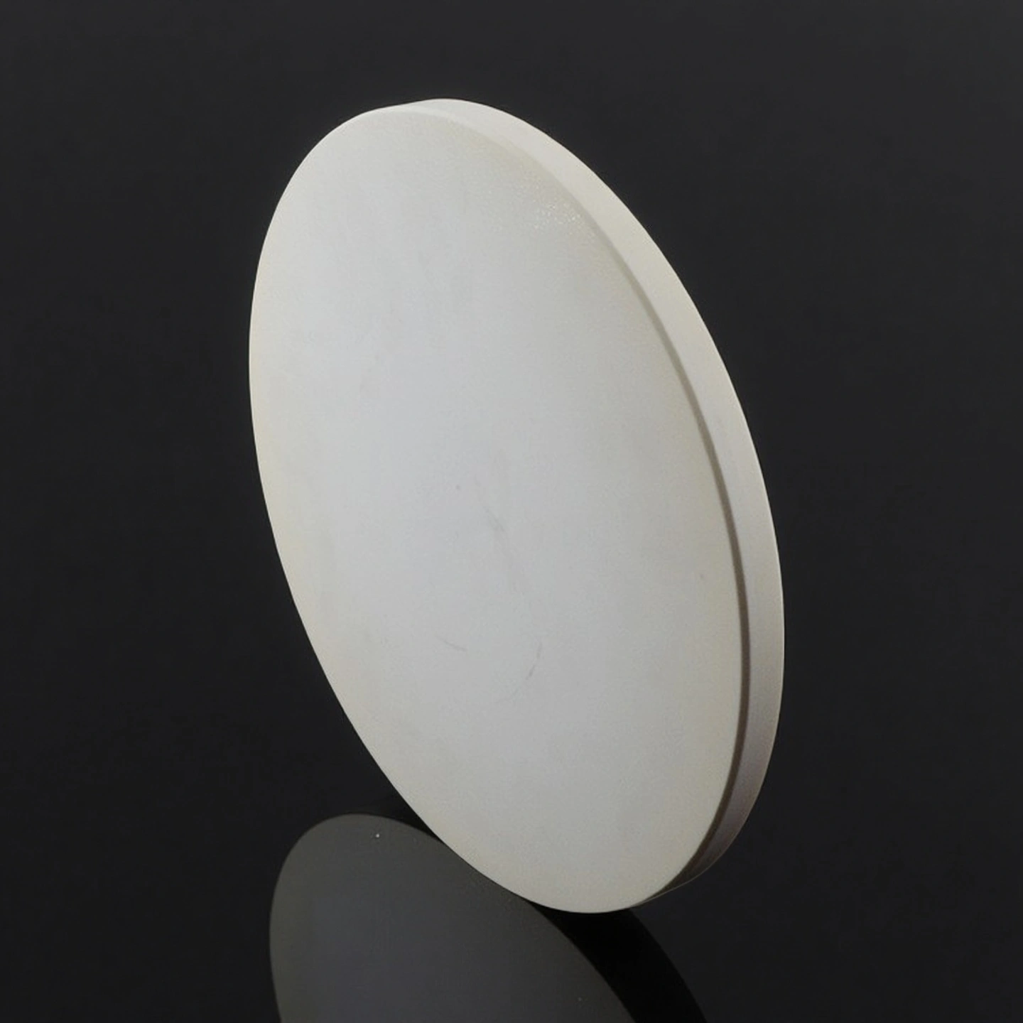
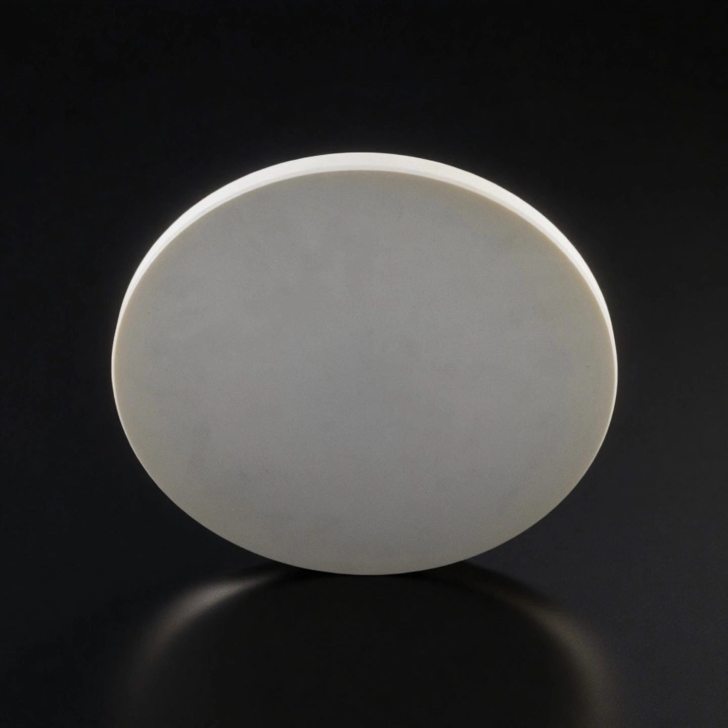
Alumina Wafer Carrier — High-Purity Ceramic Carriers, Boats, Disks and Edge Rings for Wafer Handling and Thermal Processing

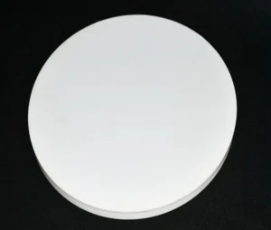
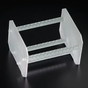
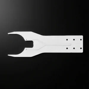
Available as carrier disks, slot boats, edge rings and loader-arm components for 4″, 6″, 8″ and 12″ (100–300 mm) wafers. Custom features include slots, pockets, holes, contact surfaces and equipment interfaces, machined to drawing with optional polished faces. Material grade is selected per drawing; property data are typical, not certified.

Catalog No. AT-BDT-B001
Material  96% -99.99% Al2O3
Max Working Temperature 1450–1800 °C
Dimensional Tolerance ±0.05–0.2 mm
Global flatness across carrier ≤1 µm (polished carrier variants)
Engineering RFQ Review
Small-Batch Custom Support
Factory-Direct Manufacturing
Drawing & Process Review

An alumina wafer carrier is a high-purity ceramic fixture—made from 99.7–99.9% alumina—designed to hold and support silicon, sapphire, and compound semiconductor wafers during processes such as diffusion, oxidation, wet cleaning, RIE and CMP. Its stable, inert structure protects wafers from deformation, particle contamination and metallic impurities while maintaining flatness through high-temperature and chemical environments.

Alumina Wafer Carrier Benefits

  • Designed for high-temperature wafer processing
    Alumina wafer carriers tolerate furnace and diffusion steps up to roughly 1700–1750 °C, allowing repeated thermal cycling without the softening or deformation seen in many polymer-based carriers.
  • Flatness and stability for polishing and lapping
    Polished alumina polishing plates and carrier plates are specified with flatness down to the micrometer and even sub-micrometer level across large diameters, supporting uniform material removal in CMP and lapping.
  • Low contamination for higher wafer yield
    Industry studies show that particulate contamination can contribute to more than 60% of wafer yield loss, so robust, low-particle carriers are critical. High-purity alumina carriers reduce organic outgassing compared with polymer boxes and contribute less micro-debris than many metal fixtures.
  • Chemically resistant in aggressive chemistries
    Alumina carrier plates withstand common wet-cleaning chemistries and CMP slurries used in wafer cleaning and polishing processes, where they are exposed to oxidizers and abrasive suspensions over long periods.
  • Flexible geometries for different tools
    Commercial alumina polishing plates and carrier plates are available as discs, rings and complex grooved forms up to several hundred millimeters in diameter, making it practical to match the fixture design to the diffusion furnace, CMP tool or cleaning bench.

Alumina Ceramic Wafer Carrier Properties

Property 96% Alumina 99% Alumina 99.5% Alumina 99.7% Alumina 99.8–99.9% Alumina
Density (g/cm³) 3.70–3.75 3.83–3.88 3.88–3.90 3.90–3.93 3.90–3.95
Hardness (GPa, typical) Approx. 14–15 Approx. 16–17 Approx. 15–18 Approx. 15–18 Approx. 15–18
Flexural Strength (MPa, typical) Approx. 260–300 Approx. 300–350 Approx. 350–380 Confirm by grade Confirm by supplier data
Typical Maximum Use Temperature (no load) 1500–1600°C 1650–1700°C Up to 1750°C 1750–1760°C Confirm by supplier data
Volume Resistivity High; electrically insulating High; electrically insulating High; electrically insulating High; electrically insulating High; electrically insulating

Alumina Wafer Carrier Specifications

Item No. Outer Dia(mm) Height(mm) Purity(%)
AT-BDT-B001 240 15 99.5
AT-BDT-B002 240 25 99.6
AT-BDT-B003 245 25 99.6
AT-BDT-B004 263 25 99.6
AT-BDT-B005 300 20 99.6
AT-BDT-B006 310 20 99.6
AT-BDT-B007 350 15 99.5
AT-BDT-B008 355 16 99.6
AT-BDT-B009 360 16 99.6
AT-BDT-B010 400 15 99

Alumina Ceramic Wafer Carrier Packaging

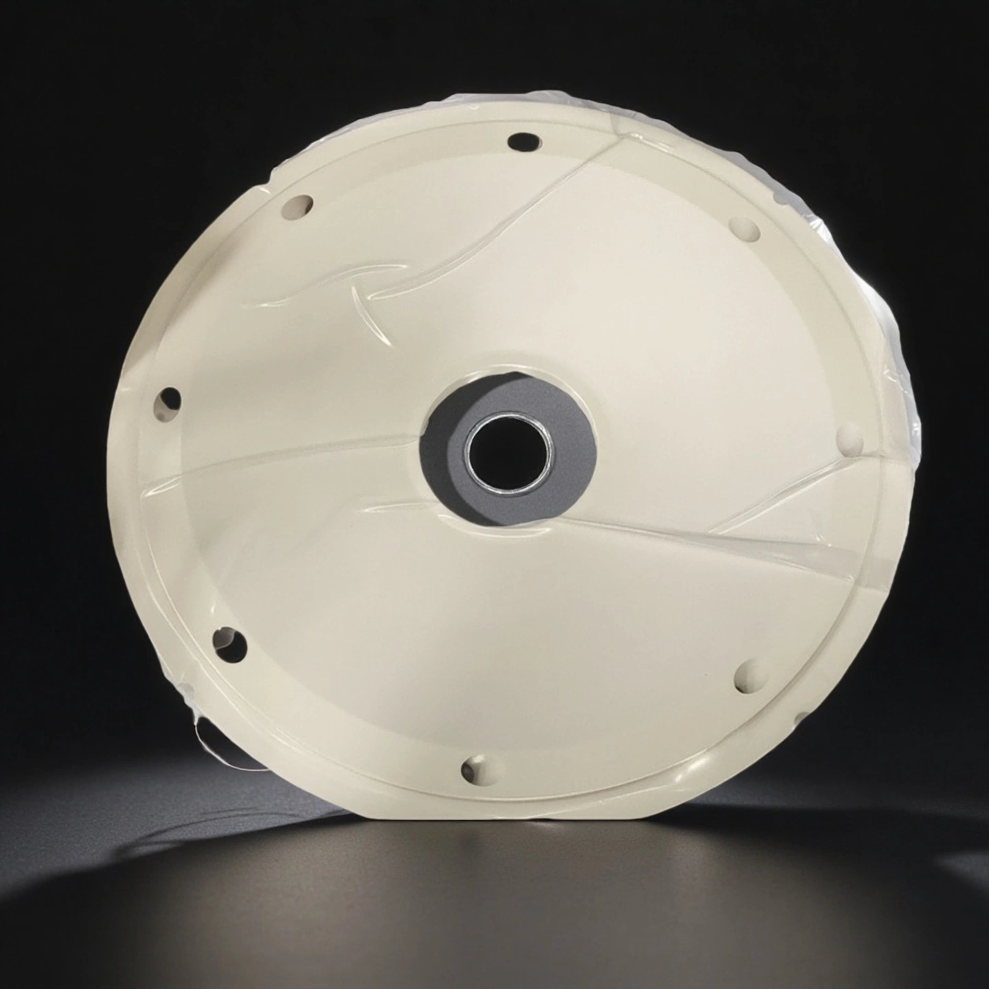
  • Carriers are first wrapped in clean, lint-free protective material to limit particle generation during transport, consistent with practices used for ceramic and polished wafer plates.
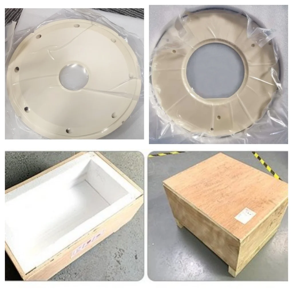
Packaging for an alumina ceramic wafer carrier

Where Alumina Wafer Carriers Are Used

Alumina wafer carriers are used when wafer support, dimensional stability, wear resistance and equipment compatibility are critical. ADCERAX custom-machines carrier disks, slot boats, edge rings, support fixtures and loader-arm components around the wafer size, contact strategy, process conditions and tool interface.

  • Wafer Handling and Automation

    Carrier disks, edge rings and ceramic loader-arm components support and locate wafers during transfer, loading, unloading and robotic handling. Contact surfaces, pockets, alignment features and clearances can be designed to help reduce backside particles, contact marks, wafer movement and edge-damage risks.

    Custom options include wafer pockets, locating pins, slots, mounting holes, vacuum features and equipment-interface details.

  • Diffusion, Oxidation and LPCVD Furnaces

    Alumina wafer boats and slot carriers can support multiple wafers through grade-dependent, high-temperature furnace processes. Compared with polymer carriers, alumina provides better dimensional stability in thermal environments where softening, outgassing or deformation may be a concern.

    Slot count, pitch, loading direction, carrier mass and support geometry can be adjusted to match the furnace layout and wafer-spacing requirements. Final material grade and temperature suitability are confirmed from the process profile and drawing.

  • Inspection, Metrology and Vacuum Support

    Flat carrier disks, support rings and custom fixtures provide defined contact points and positioning references for wafer inspection, measurement and vacuum-handling equipment. Critical datums, mounting interfaces, pockets and surface requirements can be machined to suit the inspection method.

    Ground or polished functional surfaces are available where controlled contact, positioning consistency or finished-part flatness is required. Specifications must be confirmed for each design.

  • CMP, Lapping and Wafer Cleaning

    Alumina carrier plates, polishing disks and support fixtures can be reviewed for CMP, precision lapping and wet-cleaning applications. Their hard, wear-resistant surfaces make alumina a useful candidate where the carrier is exposed to repeated contact, abrasive slurry or cleaning cycles.

    Pocket geometry, drainage features, contact areas, surface finish and chemical exposure should be defined before material and manufacturing requirements are confirmed.

  • Photovoltaic, LED and Compound-Semiconductor Processing

    Custom alumina carriers can also support wafers or fragile substrates in photovoltaic diffusion, LED processing and selected compound-semiconductor equipment. Disk, boat and fixture geometries can be adapted for different wafer formats, loading systems and thermal-process layouts.

    For non-standard wafers or fragile substrates, ADCERAX can review custom support areas, edge clearances, chip recesses and handling features from a drawing, photograph or sample.

Alumina Wafer Carrier Handling, Integration and Maintenance Guidelines

The following are general handling considerations. Final operating, cleaning and inspection procedures must be confirmed against the carrier drawing, equipment manual and process requirements.

  • Before Installation

    1. Confirm the wafer size, carrier form, pocket or slot layout, contact areas and equipment interface against the approved drawing.
    2. Check critical dimensions, mounting features and loading clearances before introducing the carrier into the tool.
    3. Inspect the carrier for visible chips, cracks, damaged pockets or surface defects that may affect wafer contact or positioning.
    4. For a new or replacement design, complete a trial installation and process validation with suitable test wafers before production use.

  • Tool Integration and Operation

    1. Load and unload wafers according to the equipment procedure, avoiding impact, forced insertion and unnecessary sliding across contact surfaces.
    2. Follow the tool manufacturer’s requirements for loading direction, alignment, temperature profile, atmosphere, vacuum and process cycle.
    3. Confirm that heating and cooling rates are suitable for the selected alumina grade and carrier geometry.
    4. Do not assume that a replacement carrier is a direct drop-in part until the dimensions, contact points and equipment interface have been validated.

  • Cleaning Process Review

    1. Define the cleaning chemistry, concentration, temperature, exposure time, rinse method and drying procedure for the specific process.
    2. Confirm compatibility between the alumina grade, surface finish and cleaning method before routine use.
    3. If ultrasonic cleaning is required, specify the solution, frequency, power and duration to avoid damaging thin sections, slots or polished surfaces.
    4. Rinse and dry the carrier according to the customer’s documented cleanliness and particle-control requirements.

  • Storage and Handling

    1. Store carriers in a clean, dry and protected location when they are not in use.
    2. Separate individual carriers with suitable protective material or dedicated racks to prevent ceramic-to-ceramic impact.
    3. Avoid direct contact with hard metal tools, sharp edges or contaminated work surfaces.
    4. Define any special handling, labeling and packaging requirements during the engineering review.

  • Inspection and Replacement Criteria

    1. Establish inspection intervals based on process cycles, wafer-contact conditions and the customer’s quality requirements.
    2. Check slots, pockets, support points, edges, mounting features and polished surfaces for wear, chips, cracks or residue.
    3. Remove and quarantine a carrier if damage could affect wafer positioning, contact conditions or equipment clearance.
    4. Confirm acceptance and replacement criteria from the approved drawing and inspection plan rather than relying only on visual judgment.

For an engineering review, provide the wafer size, carrier drawing or photographs, contact areas, equipment interface, operating temperature, atmosphere or vacuum, cleaning process and required quantity.

Alumina Wafer Carrier FAQ

  1. Q: What is an alumina wafer carrier and what forms does it come in?
    A: An alumina wafer carrier is a high-purity ceramic part that holds, locates and supports wafers during processing. Common forms are carrier disks, slot boats (wafer boats), edge rings and loader-arm parts, machined to your drawing.
  2. Q: Alumina, quartz or SiC — which wafer carrier material should I choose?
    A: Alumina suits high-temperature, chemically demanding handling and furnace support with good wear resistance and lower cost than SiC. Quartz suits certain high-purity thermal or deposition steps, and SiC suits high thermal-shock or high-conductivity duty. We advise the route at engineering review and do not present quartz or SiC performance as alumina performance.
  3. Q: What is the difference between a wafer carrier, a wafer boat and a FOUP?
    A: A carrier or boat supports and locates wafers during processing; a slot boat holds a row of wafers through furnace steps. A FOUP or plastic cassette is a room-temperature transport and storage box and is not used inside furnaces. Share your process step and we will confirm the right form.
  4. Q: What wafer sizes can an alumina wafer carrier handle?
    A: Alumina wafer carriers are typically made for 4″, 6″, 8″ and 12″ (100–300 mm) wafers, with custom designs for partial wafers, sapphire wafers and non-standard substrates. Confirm wafer size and slot layout at review.
  5. Q: What is the maximum temperature for an alumina wafer carrier?
    A: Alumina carriers and boats are typically used up to around 1700–1750 °C (no-load, grade-dependent), provided heating and cooling rates are controlled to avoid thermal shock. Reference values, not certified specifications.
  6. Q: How flat can an alumina wafer carrier be made?
    A: Polished carrier and plate variants are available for CMP, lapping and flat wafer support. We confirm the target flatness against your drawing and duty at engineering review rather than promising a fixed flatness or roughness value.
  7. Q: Can you replace or copy a worn OEM wafer carrier?
    A: We can review a backup supply from your drawing or old-part photos, confirming carrier form, wafer size, contact area and tool interface. Process validation is done by your team; we do not promise a universal drop-in replacement or direct compatibility.
  8. Q: What information do you need to quote a custom alumina wafer carrier?
    A: Wafer size, carrier type or form, drawing or old-part photos, material or purity requirement, slot count and pitch, contact area, flatness and surface expectations, thermal process and temperature, tool interface, and quantity. We review manufacturability before quotation.
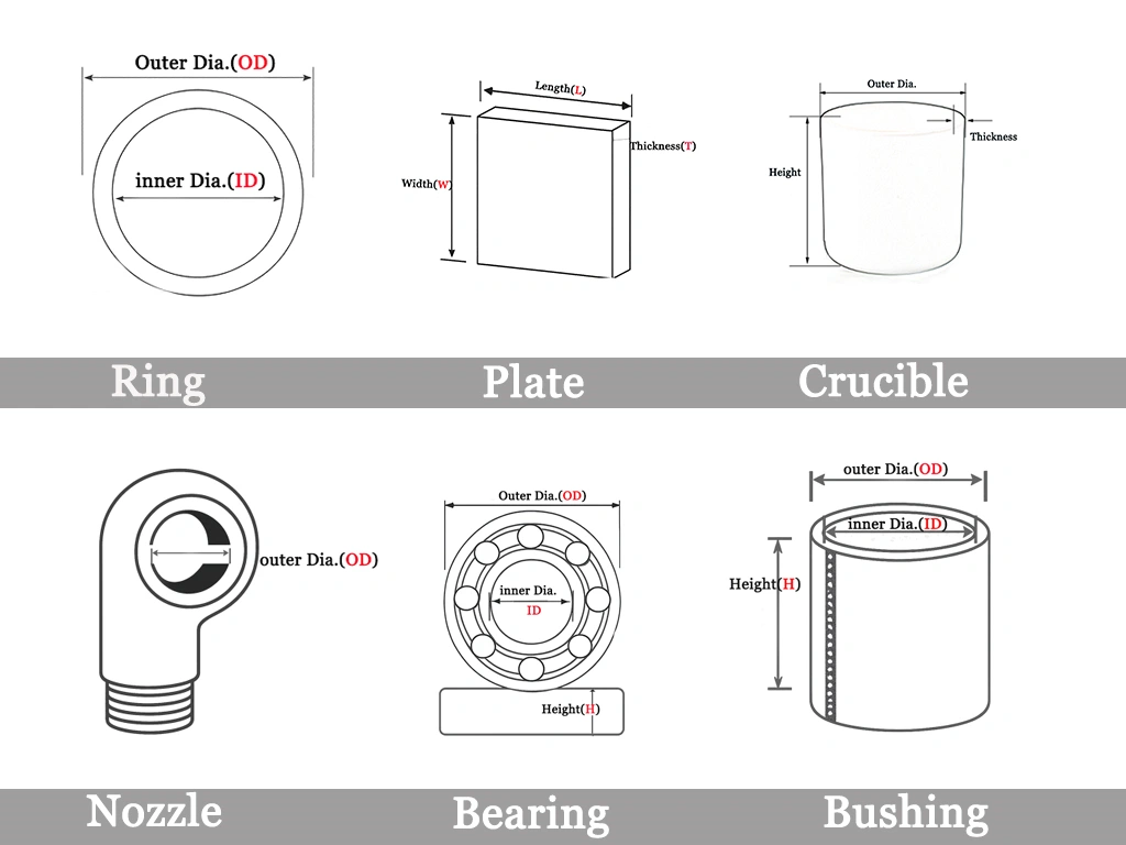
customize size

Custom Alumina Wafer Carrier

A dedicated alumina wafer carrier line allows you to match the carrier geometry, flatness and surface finish to your diffusion furnace, CMP tool or cleaning bench.

  1. Wafer size and format
    4″, 6″ and 8″ wafers, partial wafers, diced-die carriers or special formats tailored to specific tool recipes and throughput requirements.
  2. Overall carrier dimensions
    Outer and inner diameters, carrier thickness and step heights, with machining tolerances typically held within ±0.05–0.1 mm depending on geometry and wafer seating requirements.
  3. Pocket and groove patterns
    Pocket count, pocket diameter, groove width, depth and alignment layout to fit the required number of wafers, including custom chip-support recesses for fragile substrates.
  4. Carrier type and geometry
    Flat plate carriers, CMP polishing discs, ring carriers for turntables or boat-style carriers for vertical and horizontal diffusion lines, each configurable for airflow, thermal uniformity and wafer spacing control.
  5. Surface finish options
    As-sintered, fine-ground or mirror-polished surfaces, with functional faces available down to approximately 0.05 μm Ra for CMP, precision lapping or low-defect wafer support applications.
  6. Material grade selection
    Multiple alumina grades are available to match mechanical, thermal and chemical requirements. Higher grades can be selected for CMP, sapphire processing or ultra-clean wafer handling environments.
  7. Colour and identification
    White, ivory or black alumina options to support visual contrast, tool tracking, laser marking or identification coding aligned with factory automation systems.
  8. Edge, chamfer and corner details
    Custom chamfer radii, bevels and rounded edges to reduce wafer edge stress, particle generation and contact damage during high-cycle operations.
  9. Mounting and handling features
    Optional slots, tabs, notches or pin-alignment features for automated loaders, transfer robots or furnace rail systems.
  10. Thermal and structural design adjustments
    Carrier mass, ribbing structures and airflow channels can be configured to optimize heat distribution and minimize warpage during high-temperature processing.

Related Products

ADCERAX - Your Trusted Advanced Ceramics Manufacturing Partner

Direct factory manufacturing with comprehensive ceramic materials expertise and global supply capabilities

China-Based Manufacturer

ADCERAX supplies ceramic components for overseas OEMs, equipment builders, and labs.

Custom Drawing Support

We review drawings, dimensions, materials, and application conditions before quotation.

Ceramic Process Control

Forming, sintering, machining, grinding, and finishing are arranged by part requirements.

Pre-Shipment Inspection

Dimensional checks, visual inspection, and packaging review help reduce procurement risk.

Get in Touch with Us

Our team will be happy to respond to you in less than 24 hours.

Pingxiang Factory — Silicon carbide, silicon nitride, high-temperature ceramics

Quick Quotation

*Our team will answer your inquiries within 24 hours.

*Your information will be kept strictly confidential.

Ready to Solve Your Engineering Challenge?

Partner with ADCERAX for reliable, high-performance advanced ceramic solutions. Our engineers are ready to discuss your project.

E-mail

info@adcerax.com

Phone

Tel: +86-0731-84428843 WhatsApp: +86 19311583352

Response Time

Within 24 hours

An alumina wafer carrier is a high-purity ceramic fixture—made from 99.7–99.9% alumina—designed to hold and support silicon, sapphire, and compound semiconductor wafers during processes such as diffusion, oxidation, wet cleaning, RIE and CMP. Its stable, inert structure protects wafers from deformation, particle contamination and metallic impurities while maintaining flatness through high-temperature and chemical environments.

Alumina Wafer Carrier Benefits

  • Designed for high-temperature wafer processing
    Alumina wafer carriers tolerate furnace and diffusion steps up to roughly 1700–1750 °C, allowing repeated thermal cycling without the softening or deformation seen in many polymer-based carriers.
  • Flatness and stability for polishing and lapping
    Polished alumina polishing plates and carrier plates are specified with flatness down to the micrometer and even sub-micrometer level across large diameters, supporting uniform material removal in CMP and lapping.
  • Low contamination for higher wafer yield
    Industry studies show that particulate contamination can contribute to more than 60% of wafer yield loss, so robust, low-particle carriers are critical. High-purity alumina carriers reduce organic outgassing compared with polymer boxes and contribute less micro-debris than many metal fixtures.
  • Chemically resistant in aggressive chemistries
    Alumina carrier plates withstand common wet-cleaning chemistries and CMP slurries used in wafer cleaning and polishing processes, where they are exposed to oxidizers and abrasive suspensions over long periods.
  • Flexible geometries for different tools
    Commercial alumina polishing plates and carrier plates are available as discs, rings and complex grooved forms up to several hundred millimeters in diameter, making it practical to match the fixture design to the diffusion furnace, CMP tool or cleaning bench.

Alumina Ceramic Wafer Carrier Properties

Property 96% Alumina 99% Alumina 99.5% Alumina 99.7% Alumina 99.8–99.9% Alumina
Density (g/cm³) 3.70–3.75 3.83–3.88 3.88–3.90 3.90–3.93 3.90–3.95
Hardness (GPa, typical) Approx. 14–15 Approx. 16–17 Approx. 15–18 Approx. 15–18 Approx. 15–18
Flexural Strength (MPa, typical) Approx. 260–300 Approx. 300–350 Approx. 350–380 Confirm by grade Confirm by supplier data
Typical Maximum Use Temperature (no load) 1500–1600°C 1650–1700°C Up to 1750°C 1750–1760°C Confirm by supplier data
Volume Resistivity High; electrically insulating High; electrically insulating High; electrically insulating High; electrically insulating High; electrically insulating

Alumina Wafer Carrier Specifications

Item No. Outer Dia(mm) Height(mm) Purity(%)
AT-BDT-B001 240 15 99.5
AT-BDT-B002 240 25 99.6
AT-BDT-B003 245 25 99.6
AT-BDT-B004 263 25 99.6
AT-BDT-B005 300 20 99.6
AT-BDT-B006 310 20 99.6
AT-BDT-B007 350 15 99.5
AT-BDT-B008 355 16 99.6
AT-BDT-B009 360 16 99.6
AT-BDT-B010 400 15 99

Alumina Ceramic Wafer Carrier Packaging

  • Carriers are first wrapped in clean, lint-free protective material to limit particle generation during transport, consistent with practices used for ceramic and polished wafer plates.

Packaging for an alumina ceramic wafer carrier

Quick Quote

The more details you provide, the faster we can quote.

*All inquiries are confidential.

Get Your Custom Solution

The more details you provide, the faster we can respond.

customize size

*We respond within 24 hours. All inquiries are confidential.

Download Catalog