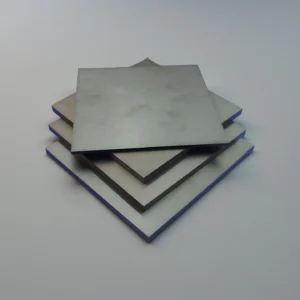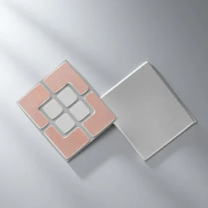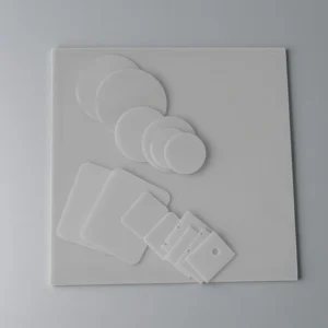
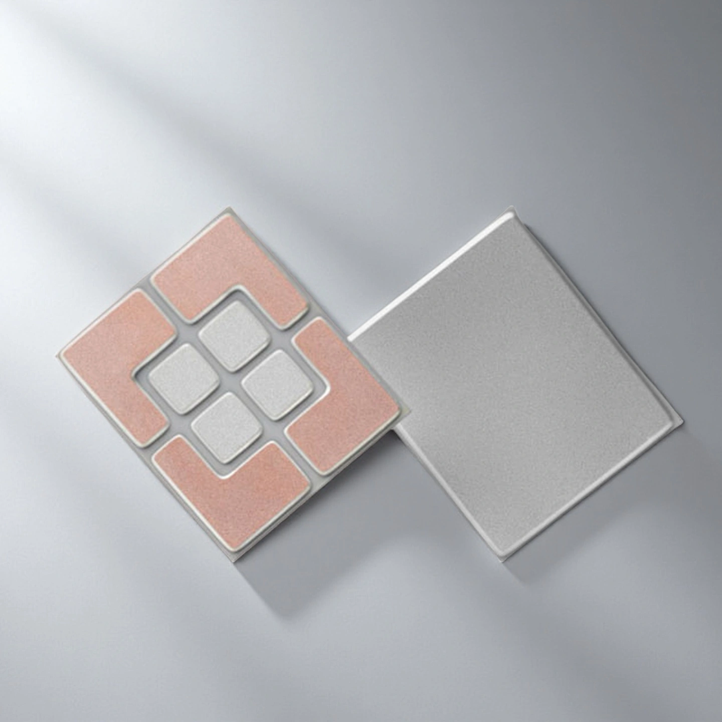
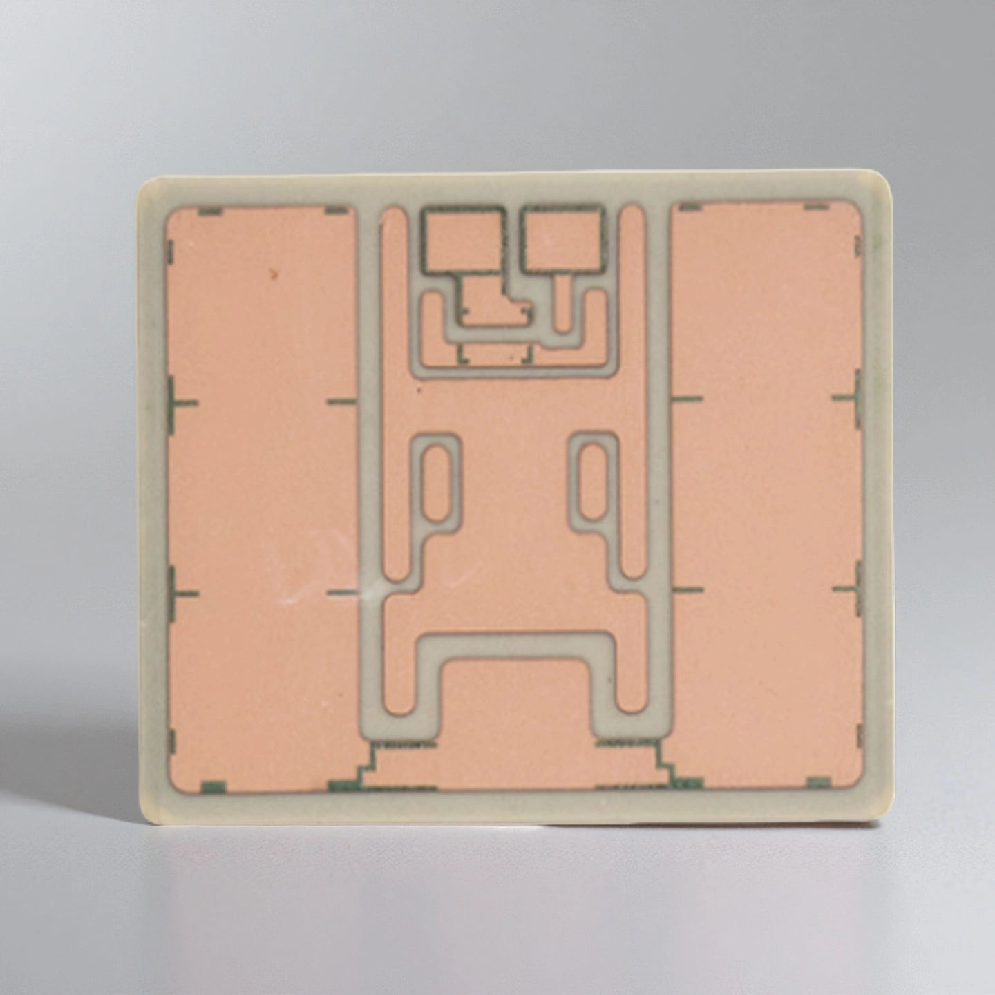
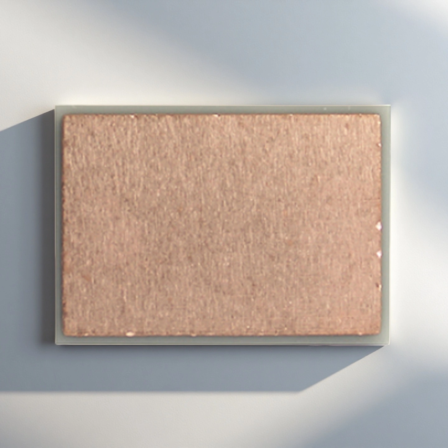
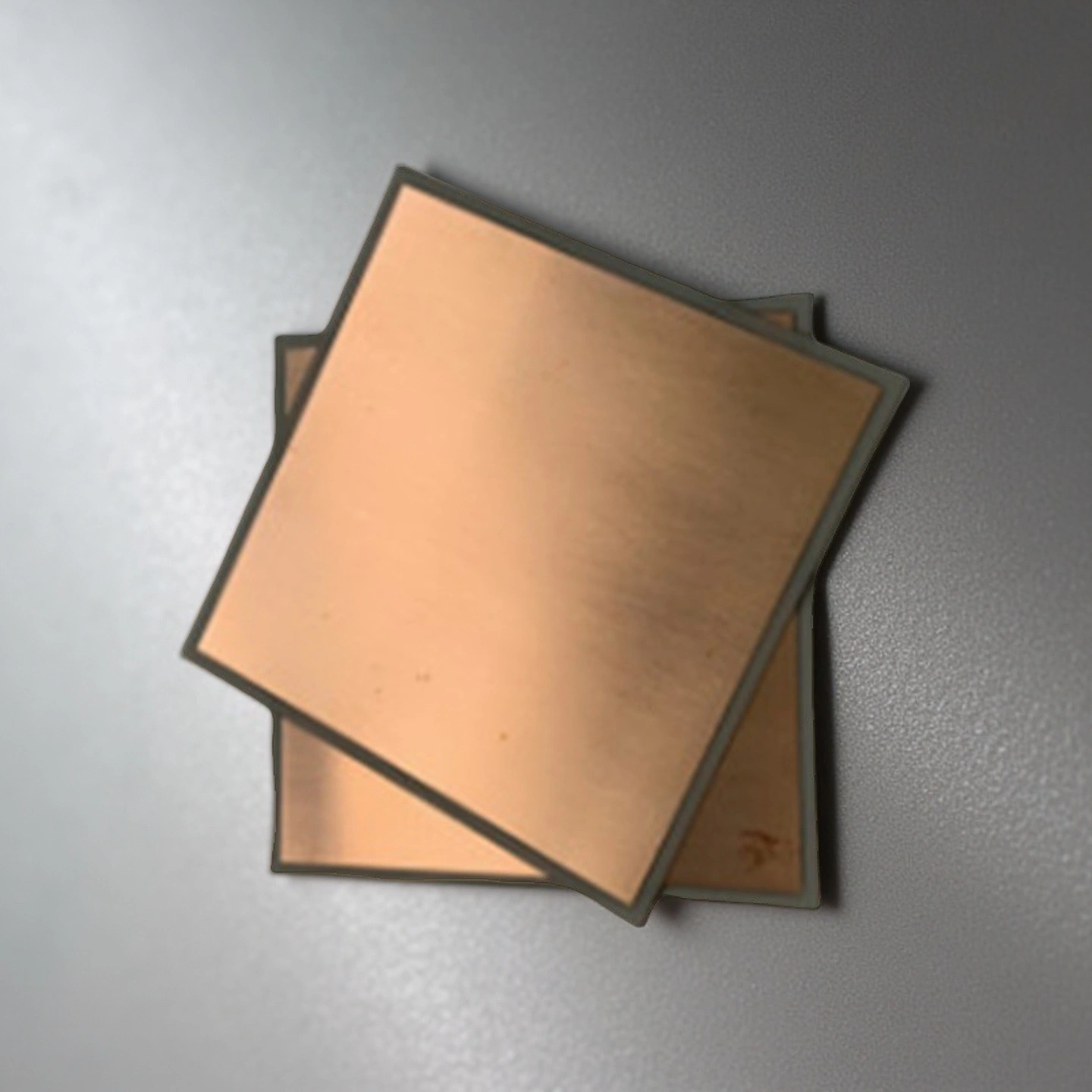
AMB silicon nitride substrate combines high thermal conductivity, low thermal expansion, and high bending strength, making it suitable for high-power semiconductor modules that undergo repeated thermal cycling. Compared with Al₂O₃ or AlN DBC substrates, silicon nitride AMB boards provide higher fracture toughness and longer power cycling life. It is widely used in traction inverters, on-board chargers, DC/DC converters, wind power converters, and industrial servo drives.
AMB Silicon Nitride Substrate Benefits
- High Power Cycling Reliability
The high fracture toughness of Si3N4 helps resist dielectric-layer cracking under SiC/IGBT thermal cycling; achievable cycle count and contact-resistance stability depend on grade, copper design and validation, not a fixed guarantee. - Low Warpage After Copper Brazing
Active metal brazing with controlled tooling helps keep panel warpage low (typically tens of microns), supporting pressure silver-sintering and uniform solder thickness; actual warpage depends on copper thickness and process. - CTE Matching with SiC Semiconductor Chips
A low CTE of about 2.7-3.2 × 10⁻⁶/K is close to SiC, which can help reduce chip-substrate thermal stress and delamination, depending on module design. - High Mechanical Strength and Crack Resistance
Si3N4 offers high flexural strength (typically 600-900 MPa by grade) and fracture toughness of approximately 6-8 MPa·m1/2, giving better edge-chip and handling resistance than more brittle Al2O3 and AlN. - Supports Thick Copper for High Current Designs
The AMB process supports about 70-500 µm copper on one or both sides for high-current, low-thermal-resistance designs; current capability depends on layout and cooling.
AMB Si₃N₄ Substrate Properties
| Si3N4 Type | Gas pressure sintering Si3N4 | Hot pressing sintering Si3N4 | High thermal conductivity Si3N4 |
| Density (g/cm3) | 3.2 | 3.3 | 3.25 |
| Flexural Strength (MPa) | 700 | 900 | 600~800 |
| Young Modulus (GPa) | 300 | 300 | 300~320 |
| Poisson's ratio | 0.25 | 0.28 | 0.25 |
| Compressive strength (MPa) | 2500 | 3000 | 2500 |
| Hardness (GPa) | 15 | 16 | 15 |
| Fracture toughness (MPa*m1/2) | 5~7 | 6~8 | 6~7 |
| Maximum working temperature (℃) | 1100 | 1300 | 1100 |
| Thermal conductivity (W/m*K) | 20 | 25 | 80~100 |
| Thermal expansion coefficient (/℃) | 3*10-6 | 3.1*10-6 | 3*10-6 |
| Thermal shock resistance (ΔT ℃) | 550 | 800 | / |
Silicon Nitride AMB Substrate Specifications
Part 1: Processing Accuracy for Silicon Nitride Substrate AMB Copper Clad
| Item | Specification | |
|---|---|---|
| Copper layer surface roughness | Ra≤1.5μm, Rz≤10μm, Rmax=50μm | |
| Coating layer | Nickel | 2-10μm (P6%-10%) |
| Silver | 0.1-1.0μm | |
| Nickel-gold | Ni: 2-10μm, Au: 0.01-0.15μm | |
| Nickel-gold-palladium | Ni: 2-10μm, Au: 0.01-0.15μm, Pd: 0.01-0.15μm | |
| Solder mask | Line width, space, tolerance | ≥0.2mm, tolerance ±0.2mm |
| Position tolerance | ±0.2mm | |
| Thickness | 5-40μm | |
| Temperature change endurance | ≤320℃/10s | |
Part 2: AMB Silicon Nitride Substrate Size
| AMB Silicon Nitride Substrate | |||
| Item No. | Length*Width(mm) | Thickness(mm) | Copper layer thickness(mm) |
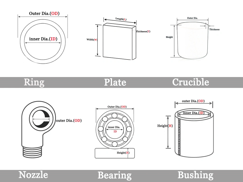
| AT-SIN-FT1001 | 10*10——127*178 | 0.25 | 0.127、0.2、0.25、0.3、0.4、0.5、0.8 |
| AT-SIN-FT1002 | 0.32 | ||
| AT-SIN-FT1003 | 0.38 | ||
| AT-SIN-FT1004 | 0.63 | ||
| AT-SIN-FT1005 | 1.0 | ||
| AT-SIN-FT1006 | Other thickness customization | ||
AMB Si₃N₄ Substrate Packaging
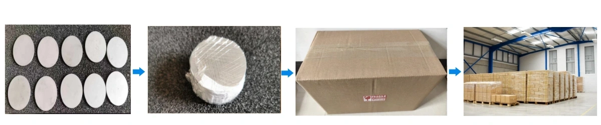
- Each Si3N4 active metal brazed substrate is sealed in anti-static packaging.
- Packed in foam-lined boxes to prevent mechanical damage.