Guides for alumina substrate properties, thickness selection, thin-film use, cleaning, etching, and comparison with FR4. For electronics and equipment engineers specifying substrate dimensions, surface finish, and metallization readiness.
ADCERAX Ceramics Catalog
Materials, product forms, and capabilities in one PDF.
Alumina Substrate Etching often emerges when reliable surfaces suddenly fail to bond, pattern, or endure service stresses, thereby disrupting downstream
Alumina Substrate choices often surface when FR4 begins to saturate thermal headroom, insulation margins, or lifetime targets. Consequently, this comparison
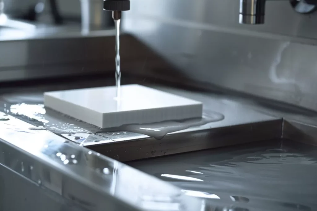
Al2O3 Substrate Cleaning often begins only after process failures appear; however, delayed intervention typically magnifies adhesion loss, electrical instability, and
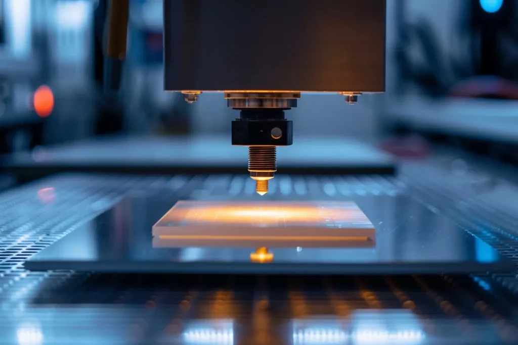
In advanced thin-film manufacturing, the alumina substrate serves as the foundational platform upon which electrical, thermal, and mechanical behaviors are
Alumina Substrate decisions often begin under uncertainty, where material failure risks, thermal limits, and long-term stability remain unclear during early
Alumina Substrate Properties define whether electronic systems endure thermal stress or fail prematurely. Consequently, overlooking material behavior often results in
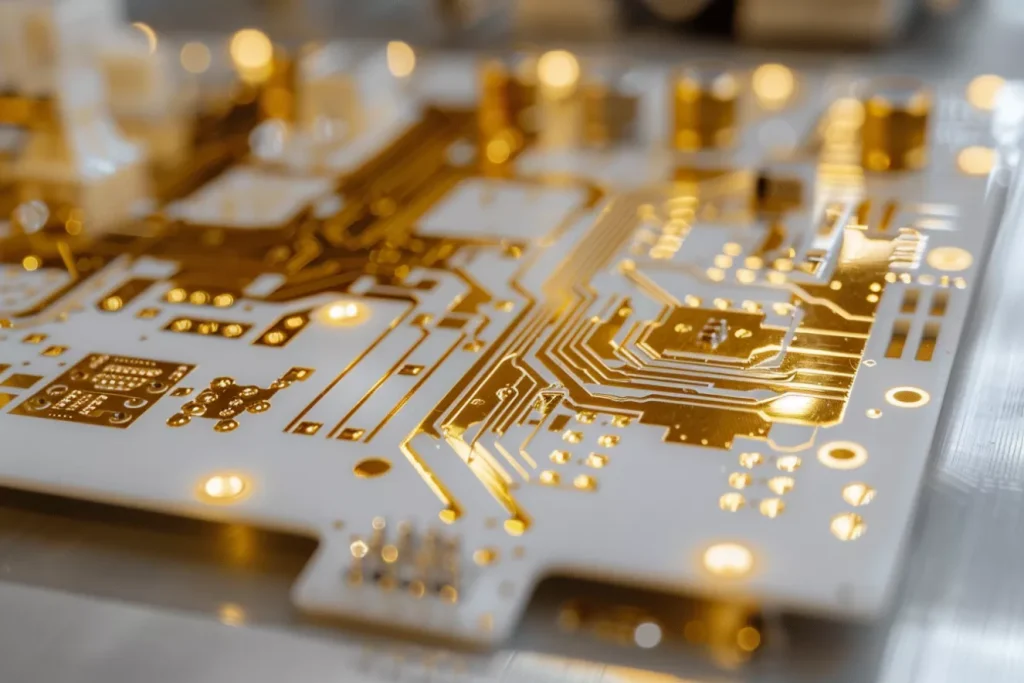
Alumina Substrate selection often determines whether a PCB can withstand heat, electrical stress, and long-term operation. However, many electronic failures
Need help selecting the right ceramic for your application?
Send your drawing, material requirement, dimensions, quantity, and working conditions — our engineering team reviews manufacturability before quotation.