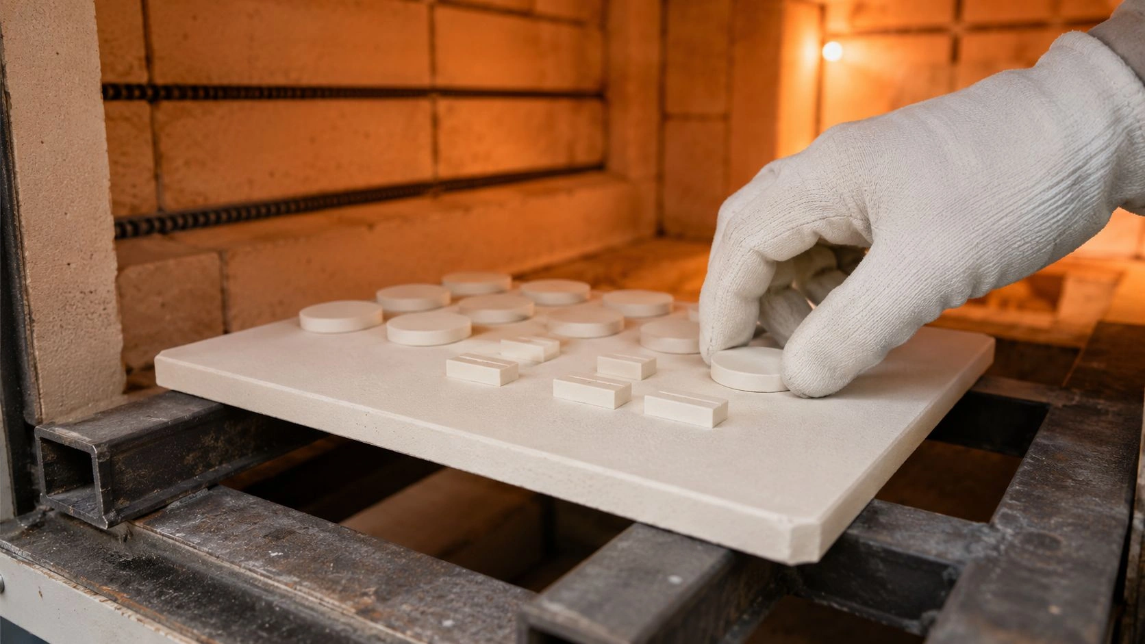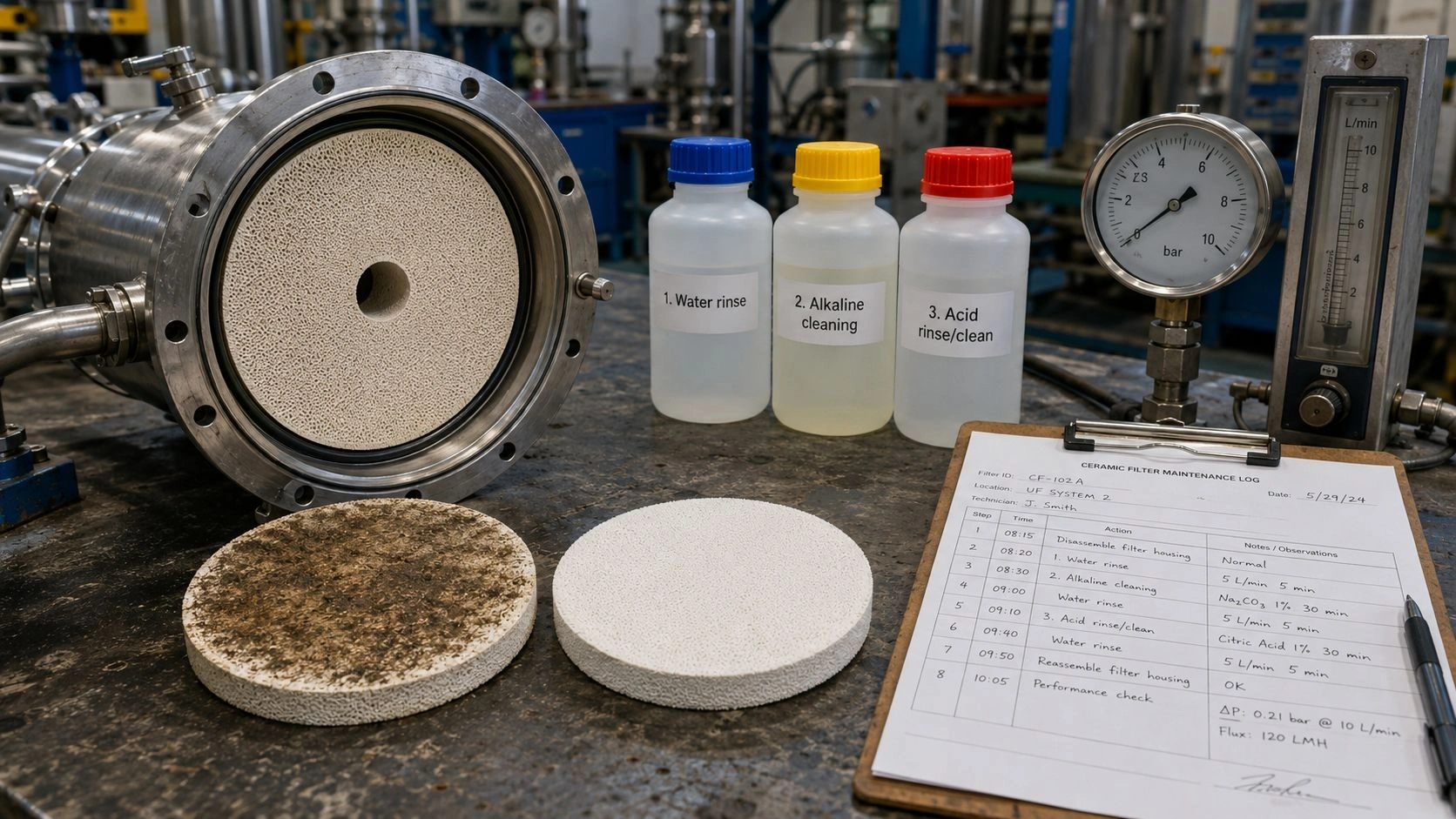
Alumina substrate etching is a surface-engineering step used when metallization adhesion, bonding anchorage, microstructuring, or rework cleanup needs a controlled interface — without treating etch as a universal fix for bulk ceramic limits.
This guide walks process windows for chemical, physical, and hybrid routes, then maps them to metallization/bonding RFQ fields (grade class, target Ra, stackup, coupon peel, lead time). Ranges below are illustrative / application-typical screening — confirm chemistry, metrology, and coupon results on RFQ.
Start from why etch appears, then material response, method trade-offs, reliability checks, and when etching should be skipped. For grade and form-factor context, see alumina substrates; for etch window · Ra · metallization RFQ support, see custom ceramic services and materials.
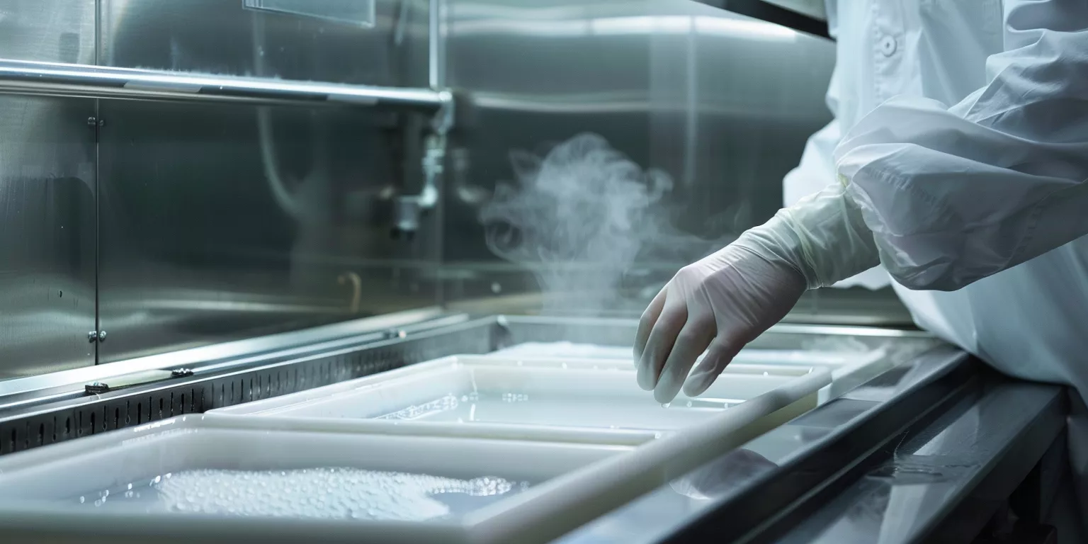
Before examining specific methods, it is essential to clarify why Alumina Substrate Etching appears repeatedly across otherwise mature ceramic manufacturing lines, particularly when performance targets tighten.
Why Etching Becomes Necessary in Alumina Substrate Processing
Alumina substrates are inherently stable, electrically insulating, and dimensionally reliable; however, these same attributes often limit surface interaction with metals, coatings, or bonding agents. Consequently, etching is introduced as a controlled intervention rather than a default step, enabling functional interfaces without altering bulk properties.
-
Interface performance limitations become visible at scale
In many production environments, alumina substrates initially perform acceptably without surface modification. Nevertheless, as thermal cycling duty and metallized-layer thickness increase, adhesion variability can become evident. Published-range and plant screening often show peel strength drop after cycling when surface engagement is weak — treat any % figure as illustrative; confirm stackup · metallization · coupon peel on RFQ (not a contract adhesion SLA). -
Geometric and functional integration demands increase
As circuit densities rise and mechanical tolerances tighten, flat alumina surfaces no longer provide adequate anchoring for deposited films or bonded structures. Specifically, micro-scale surface features on the order of 1–5 μm become necessary to stabilize interfaces without compromising electrical insulation. Etching offers a pathway to introduce such features in a controlled manner. -
Manufacturing recovery and lifecycle extension require intervention
During rework or failure analysis, residual metallization or contamination layers must often be removed without damaging the ceramic base. In these cases, selective etching becomes the only viable option to restore substrate usability while maintaining dimensional integrity within ±0.05 mm.
Consequently, etching transitions from an optional enhancement to a strategic tool that reconciles material stability with functional adaptability, thereby setting the stage for deeper exploration of alumina surface behavior and processing pathways in the sections that follow.
Material Structure of Alumina Substrates and Etching Responsiveness
Before any etching pathway is evaluated, the intrinsic material structure of alumina substrates establishes clear boundaries on how surfaces respond to chemical or physical modification. Consequently, understanding microstructural behavior is essential for predicting etching outcomes and avoiding unintended degradation.
-
Polycrystalline grain structure governs local etching variability
Alumina substrates are typically polycrystalline, composed of tightly packed grains ranging from 1 to 10 μm depending on sintering conditions. As a result, etching reactions rarely proceed uniformly across the surface; instead, grain boundaries exhibit higher chemical activity than grain interiors. In practice, engineers often notice preferential material removal along these boundaries, leading to micro-topographical contrast rather than smooth planar recession. This behavior explains why alumina etching enhances surface engagement without producing deep, silicon-like features. -
Purity level directly influences chemical stability and reaction window
Industry-typical electronic substrate classes are often discussed as ~96% and ~99% Al₂O₃ (screening language — not a single catalog SKU guarantee; supplier grade sheets may list 95% / 99.x% families). Glassy phases or sintering aids soften or dissolve earlier during chemical exposure, accelerating localized removal. Higher-purity classes show slower etch kinetics and narrower windows. Identical recipes can therefore yield different surface states across grade classes — confirm grade · chemistry · metrology on RFQ. -
Surface energy and porosity define etching responsiveness rather than bulk hardness
Although alumina exhibits high hardness values exceeding 1500 HV, etching behavior correlates more strongly with surface energy distribution and closed porosity than with bulk mechanical strength. Minor variations in surface finish or residual porosity can alter etch rates (illustrative order often cited around tens of percent) under otherwise identical conditions — confirm on process DOE. Consequently, surface preparation steps prior to etching often determine final reproducibility more than the etching medium itself. This insight shifts engineering focus from aggressiveness to consistency.
Taken together, alumina substrate etching is fundamentally constrained by microstructural realities, which means subsequent process selection must respect material-driven limits rather than relying on generalized ceramic assumptions.
Chemical Etching Mechanisms Applicable to Alumina Substrates
Chemical etching represents the most frequently evaluated pathway when controlled surface modification of alumina is required. Moreover, it offers predictable interaction with microstructural features while preserving bulk integrity, provided that reaction parameters remain within defined boundaries. Accordingly, understanding chemical mechanisms becomes essential before considering hybrid or physical alternatives.
Acid-Based Etching Systems and Their Reaction Pathways
Chemical interaction between alumina and acidic media occurs primarily through surface hydroxyl groups rather than bulk dissolution. Consequently, etching progresses slowly and selectively; published/illustrative rates often sit near ~0.1–0.5 μm/min under controlled lab conditions — confirm acid · concentration · T · agitation on process DOE (not a factory etch-rate SLA).
In industrial practice, phosphoric-acid-based systems at elevated temperatures (OEM-/chemistry-dependent screening often cited near ~180–280 °C) are frequently reported. They preferentially attack glassy grain-boundary phases, producing application-typical roughness moves from polished baselines toward roughly Ra ~0.8–1.5 μm when grade · chemistry · metrology are controlled — not a global Ra SLA. Extending exposure beyond short pilot windows (often ~10–15 min in published screening) can yield diminishing roughness gains while raising defect probability — confirm recipe on RFQ. This balance highlights why alumina etching relies on boundary activation rather than aggressive bulk removal.
Therefore, acid-based etching should be viewed as a surface activation mechanism rather than a material removal strategy, particularly when dimensional preservation is critical.
Selectivity Control and Etch Rate Stability
Etch selectivity in alumina substrates is governed by phase distribution rather than crystallographic orientation. As a result, industry-typical ~96% class substrates often etch faster than ~99% class variants under identical baths — illustrative deltas commonly cited around tens of percent and are glass-phase dependent (96% class ≠ a fixed catalog SKU). Confirm grade sheet + DOE; do not treat as a contract rate ratio.
During scaled processing, tight thermal uniformity (OEM-dependent; screening often cites about ± a few °C) is essential for uniform surface evolution. Uneven batch heating can introduce roughness scatter that hurts metallization adhesion consistency — confirm thermal map on process RFQ. Engineers therefore emphasize thermal uniformity and agitation control as primary stability levers. Chemical concentration alone rarely compensates for thermal inconsistency in alumina etching.
Consequently, repeatable etching outcomes depend more on process environment control than on increasing chemical aggressiveness.
Chemical Etching Risks Including Microcrack Initiation
Although chemical etching is comparatively gentle, excessive exposure can initiate microstructural damage. Specifically, prolonged boundary dissolution weakens grain interlocking, increasing the probability of microcrack formation under subsequent thermal cycling.
Screening observations indicate that over-long high-temperature acid exposure can reduce flexural strength (illustrative published-range often cited ~8–15%) — screening only, not a contract strength-loss %. Changes may stay invisible optically yet show up in thermal-shock qualification; confirm mechanical coupon plan on RFQ. Engineers encountering unexpected fracture frequently trace failures back to overly extended etching steps. This experience reinforces the importance of conservative exposure windows.
Thus, chemical etching must be bounded by mechanical reliability considerations rather than surface appearance alone.
Chemical etching — illustrative / OEM-dependent screening (confirm process DOE + RFQ)
| Parameter | Illustrative screening window |
|---|---|
| Etch rate (μm/min) | ~0.1–0.5 (illustrative; DOE-dependent) |
| Operating temperature (°C) | ~180–280 (OEM-/chemistry-dependent) |
| Application-typical Ra move (μm) | ~0.6–1.3 (grade · chemistry · metrology) |
| Flexural screening risk | Over-etch can reduce strength (screening only; no contract %) |
| Exposure time (min) | ~5–15 pilot screening |
| Grade-class sensitivity | High (glass-phase dependent) |
| Dimensional impact | Usually small when controlled |
Table values are published-range / application-typical screening — not acceptance SLAs.
Physical and Hybrid Etching Approaches for Alumina Substrates
While chemical etching addresses surface activation through controlled reactions, physical and hybrid approaches are adopted when spatial selectivity or pattern definition becomes critical. Moreover, these methods enable localized modification without immersing the entire substrate in reactive environments. Accordingly, engineers evaluate physical and hybrid etching as complementary tools rather than direct replacements for chemical processes.
Laser-Based Surface Texturing on Alumina Substrates
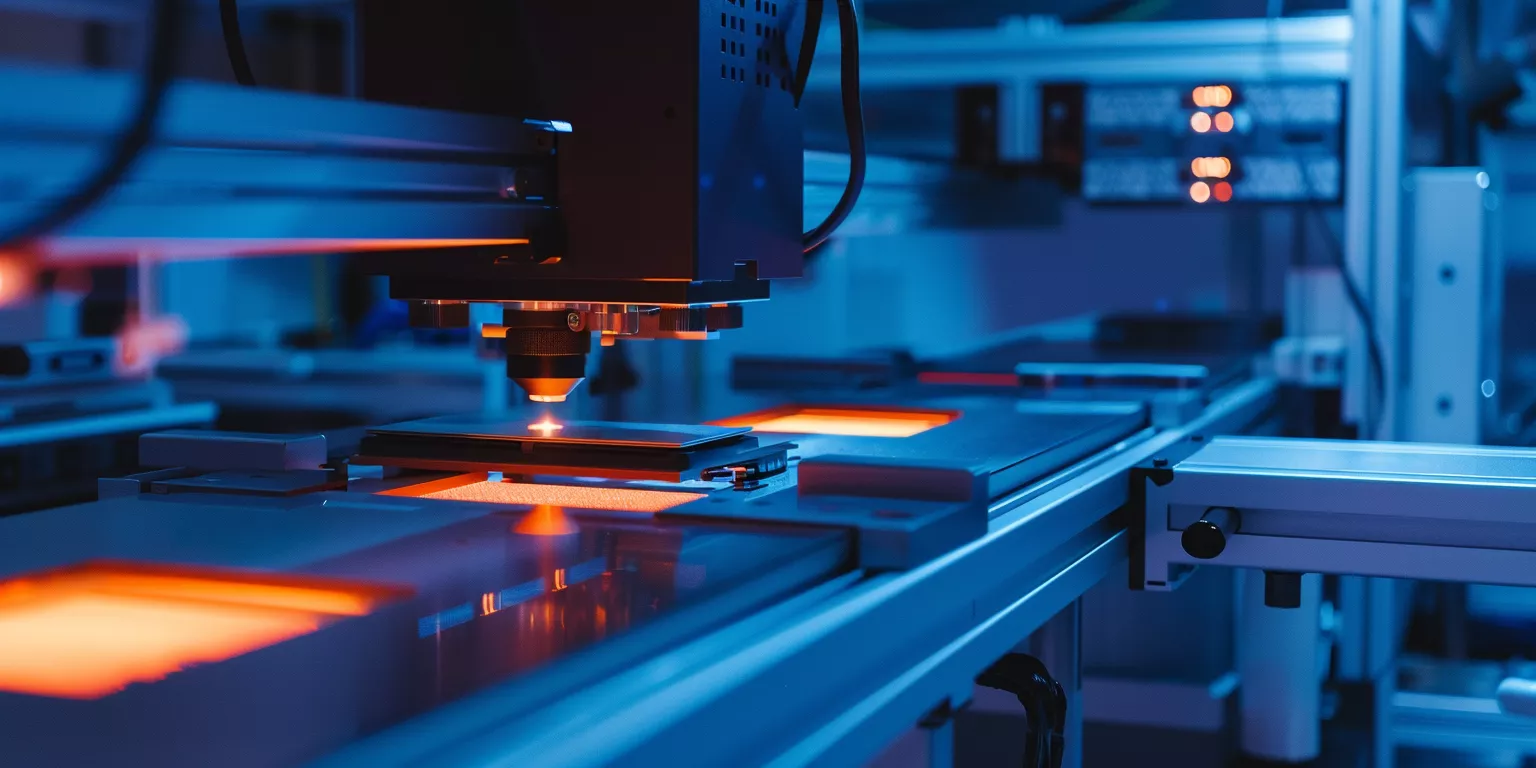
Laser-based texturing modifies alumina surfaces through localized thermal and ablation effects rather than chemical dissolution. Consequently, material interaction is confined to precisely defined regions, often within 10–50 μm spot diameters.
In industrial settings, pulsed laser systems operating between 10–100 ns pulse widths are commonly applied to generate microgrooves or anchor patterns. Equipment-dependent capability screening often cites feature depths around ~2–20 μm, depending on energy density and scan speed. Improper parameters can introduce heat-affected zones (illustrative ~3–8 μm) that may alter local dielectric behavior — confirm laser process RFQ. This sensitivity explains why laser etching demands tight parameter envelopes rather than broad process margins.
Therefore, laser texturing is most effective when feature placement outweighs concerns about subsurface thermal alteration.
Abrasive and Plasma-Assisted Methods
Abrasive-based techniques, including micro-blasting and controlled grit projection, rely on mechanical impact rather than thermal or chemical interaction. As a result, surface roughness can rise rapidly (equipment-dependent screening often cites Ra ~1.5–3.5 μm) within short exposures — confirm blast media · pressure · time on RFQ.
Plasma-assisted treatments, by contrast, alter surface chemistry and energy without significant material removal. In practice, plasma exposure modifies only the upper tens–hundreds of nm while soft-illustrative wetting gains are sometimes cited; treat wetting % as softened illustrative — confirm contact-angle method on RFQ. Engineers often combine light abrasive texturing with plasma activation to balance anchoring depth and cleanliness. This hybrid sequencing reduces particle embedment risks commonly observed in standalone abrasive processing.
Accordingly, abrasive and plasma methods are selected when speed and surface activation outweigh the need for fine geometric control.
Comparative Process Windows Between Chemical and Physical Etching
Physical and chemical etching differ fundamentally in how process windows are defined. Chemical systems rely on temperature, concentration, and time, whereas physical methods depend on energy density, exposure duration, and tool stability.
During pilot evaluations, engineers frequently observe that chemical etching maintains dimensional deviation below ±0.02 mm, while aggressive physical methods may exceed ±0.05 mm without masking strategies. Nevertheless, physical etching achieves localized modification unattainable through immersion processes. This contrast drives hybrid adoption when both dimensional control and localized roughening are required.
Consequently, comparative selection hinges on whether uniformity or spatial precision represents the dominant design constraint.
Physical / hybrid etching — equipment-dependent capability screening (confirm process RFQ)
| Approach | Feature depth screening (μm) | Ra screening (μm) | HAZ screening (μm) | Spatial selectivity | Dimensional stability |
|---|---|---|---|---|---|
| Laser texturing | 2–20 | 0.8–2.0 | 3–8 | High | Moderate |
| Abrasive micro-blasting | 5–30 | 1.5–3.5 | None | Low | Low |
| Plasma-assisted treatment | <0.2 | <0.5 | None | Moderate | High |
| Hybrid abrasive + plasma | 3–15 | 1.0–2.5 | None | Moderate | Moderate |
Etched Alumina Surfaces for Metallization and Film Deposition
Etched alumina surfaces play a decisive role in metallization and film deposition performance, particularly where electrical reliability and thermal endurance intersect. Moreover, surface modification directly influences interfacial adhesion mechanisms that cannot be compensated by deposition parameters alone. Accordingly, etching is treated as a prerequisite step rather than a corrective measure in advanced alumina-based assemblies. For finished metalized builds, see also metalized alumina ceramic substrates.
Etching-Induced Roughness and Metallization Adhesion Strength
Surface roughness generated through etching establishes mechanical interlocking between alumina substrates and deposited metallic layers. Consequently, adhesion improvements arise from geometric anchoring rather than chemical bonding alone.
Published-range and application-typical screening often place useful metallization windows near Ra ~0.8–1.5 μm, with adhesion / peel improvements reported versus unetched baselines. Treat peel N·mm⁻¹ and adhesion % as illustrative / published-range screening — confirm stackup · metallization system · coupon peel on RFQ; not contract N/mm or %. Roughness far above application windows can introduce stress raisers. Adhesion gains plateau beyond an application-typical roughness band.
Therefore, etching parameters must target controlled micro-topography rather than maximal surface aggression.
Compatibility with Mo-Mn and Thin-Film Metallization Systems
Mo-Mn metallization1 remains widely used for alumina substrates due to its thermal compatibility and proven reliability. Consequently, etched surfaces must support uniform paste wetting and sintering behavior without trapping residual contaminants.
During pilot production, etched alumina can improve Mo-Mn continuity after high-temperature firing (recipe-dependent). Thin-film sputtering may show fewer pinholes when nucleation is more uniform — treat defect-% deltas as illustrative; confirm on coupon builds. These outcomes demonstrate that etching influences deposition morphology as much as adhesion strength.
Thus, metallization compatibility depends on how etching modifies both surface energy and micro-scale geometry.
Thermal Cycling Reliability of Etched and Metallized Alumina Substrates
Thermal cycling performance remains the decisive qualification metric for metallized alumina substrates. Consequently, etched interfaces must maintain integrity under repeated expansion and contraction cycles.
In accelerated testing, etched and metallized alumina substrates consistently withstand 500–1000 thermal cycles between −40 °C and 150 °C with less than 5% adhesion degradation. By contrast, non-etched substrates often exhibit early edge lifting or microcrack initiation after 200–300 cycles. Engineers conducting failure analysis frequently trace these differences to interfacial stress redistribution enabled by etched surface features. This correlation reinforces etching as a reliability enabler rather than a cosmetic enhancement.
Accordingly, thermal endurance validation should always consider surface preparation history alongside metallization design.
Metallization screening comparison — illustrative / published-range (confirm coupon peel RFQ)
| Parameter | Unetched (screening) | Etched (screening) |
|---|---|---|
| Application-typical Ra (μm) | ~0.1–0.3 | ~0.8–1.5 (grade · chemistry · metrology) |
| Peel / adhesion | Lower interlocking | Illustrative published-range gains; confirm N·mm⁻¹ on coupon — no contract % |
| Thin-film defect trend | Baseline | Often improved nucleation (illustrative) |
| Thermal-cycle example | Earlier edge risk in some stacks | Hypothetical/application-dependent; confirm qual plan — no life SLA |
| Delamination risk trend | Higher when smooth | Lower when Ra window matched |
| Reproducibility | Surface-limited | Better when process DOE locked |
No contract peel N/mm, adhesion %, or cycle life guarantees — RFQ + coupon.
Microstructuring Alumina Substrates Through Etching
Microstructuring through etching addresses application scenarios where alumina substrates must perform beyond planar support functions. Moreover, controlled surface features enable functional integration in sensing, fluid handling, and interface management without altering bulk ceramic properties. Accordingly, etching-based microstructuring is evaluated as a surface-level engineering solution rather than a bulk material transformation.
Formation of Microgrooves and Controlled Surface Features
Etching enables the formation of shallow microgrooves and textured regions that guide mechanical, thermal, or fluid interactions. Consequently, feature generation remains constrained to surface layers while preserving structural rigidity.
In practical implementations, chemical and hybrid routes yield shallow microgrooves (equipment-/mask-dependent screening often ~1–8 μm depth and ~10–50 μm width). Sensor housings often prefer shallow textures to limit stress concentration; deeper attempts can go irregular due to grain-boundary dominance — confirm feature DOE on RFQ. This limitation underscores the surface-oriented nature of alumina microstructuring.
Therefore, etched microfeatures are best applied for guidance and anchoring rather than volumetric shaping.
Etching Limitations Imposed by Alumina Brittleness
Alumina’s intrinsic brittleness imposes strict limits on how aggressively microstructuring can be pursued. As a result, etching cannot replicate deep, high-aspect-ratio features common in silicon processing.
Field experience shows that when etched feature depth pushes past shallow screening windows, localized stress can raise crack initiation risk during mechanical or thermal loading — treat % risk deltas as illustrative; confirm mechanical coupon plan. Engineers evaluating failed microstructured substrates often observe crack paths following etched boundary regions rather than bulk grain interiors. This behavior clarifies why alumina microstructuring must remain shallow and conservative.
Accordingly, successful designs emphasize distributed microtextures instead of isolated deep cavities.
Functional Integration in Microfluidic and Sensor Interfaces
Microstructured alumina substrates are increasingly adopted in sensor and microfluidic interfaces where chemical stability and insulation are critical. Consequently, etched textures serve as alignment aids, flow stabilizers, or bonding anchors.
In microfluidic testing environments, etched patterns can improve wetting consistency (softened illustrative gains sometimes cited); confirm fluid · contact-angle method on RFQ rather than treating % as a contract KPI. Sensor developers similarly report improved repeatability when etched regions localize active elements without introducing electrical leakage paths. These outcomes demonstrate that microstructuring enhances functional integration without compromising alumina’s inherent insulation.
Thus, etching-based microstructuring aligns well with precision-oriented applications rather than load-bearing roles.
Microstructuring — equipment-dependent capability screening
| Aspect | Illustrative screening |
|---|---|
| Microfeature depth (μm) | ~1–8 (confirm DOE) |
| Lateral feature width (μm) | ~10–50 |
| Crack-risk depth trend | Risk rises as features deepen past shallow windows |
| Wetting consistency | Softened illustrative improvement — confirm method |
| Electrical insulation impact | Usually none when residue-controlled |
| Structural integrity | Keep features shallow vs bulk strength needs |
Etching in Rework Cleaning and Failure Analysis Contexts
Etching assumes a different function in rework and failure analysis, where the objective shifts from surface enhancement to controlled material removal. Moreover, these contexts demand extreme selectivity, as the alumina substrate must remain structurally intact while unwanted layers are eliminated. Accordingly, etching is applied as a precision recovery tool rather than a surface optimization step.
Selective Removal of Residual Metallization Without Substrate Damage
In rework scenarios, etching is often used to remove residual metallization layers while preserving the underlying alumina substrate. Consequently, process windows are deliberately narrow to avoid unintended ceramic attack.
During controlled rework, illustrative metal-removal rates often sit near ~0.2–0.6 μm/min with short exposure windows — confirm chemistry · T · time on process DOE. Over-exposure can push Ra into ranges that complicate re-metallization (application-typical caution near ~Ra 2 μm). Successful rework therefore relies on time-limited exposure rather than aggressive chemistry.
Thus, selective etching enables substrate reuse while maintaining dimensional and surface consistency.
Surface Artifacts Introduced by Improper Etching Practices
Improper etching conditions frequently introduce artifacts that obscure failure analysis rather than clarify it. As a result, analysts must distinguish between process-induced damage and original failure signatures.
In laboratory investigations, over-etched alumina surfaces exhibit boundary pitting and microvoid formation measurable at 1–3 μm depth. Engineers conducting root-cause analysis often report misinterpretation when these artifacts mimic crack initiation sites. Such false indicators can lead to incorrect conclusions regarding metallization or thermal fatigue failures.
Accordingly, controlled etching protocols are essential to preserve diagnostic clarity during failure analysis.
Etching as a Diagnostic Preparation Step
Beyond material removal, etching is frequently employed to expose hidden interfaces for inspection. Consequently, it supports microscopy and cross-sectional evaluation without mechanical polishing.
In failure analysis workflows, light etching enhances interface visibility by increasing contrast between alumina grains and residual layers. Analysts often report clearer crack-path identification when light etch preparation replaces dry polishing — treat accuracy % as illustrative. This approach minimizes mechanical smearing while preserving microstructural authenticity.
Therefore, etching functions as an enabling step that improves analytical resolution rather than altering failure mechanisms.
Rework / FA etching — illustrative control screening (confirm DOE)
| Context | Primary objective | Illustrative screening |
|---|---|---|
| Metallization rework | Remove metal layers | ~0.2–0.6 μm/min (DOE-dependent) |
| Exposure duration | Limit ceramic attack | Short windows; confirm recipe |
| Artifact depth | Avoid false FA markers | Keep shallow vs diagnostic risk |
| Post-rework Ra | Re-metallization readiness | Stay within application-typical limits |
| Diagnostic clarity | Interface exposure | Often improved vs dry polish (illustrative) |
| Substrate reuse | Post-rework | Feasible when controlled |
Etched Alumina Surfaces and Structural Bonding Performance
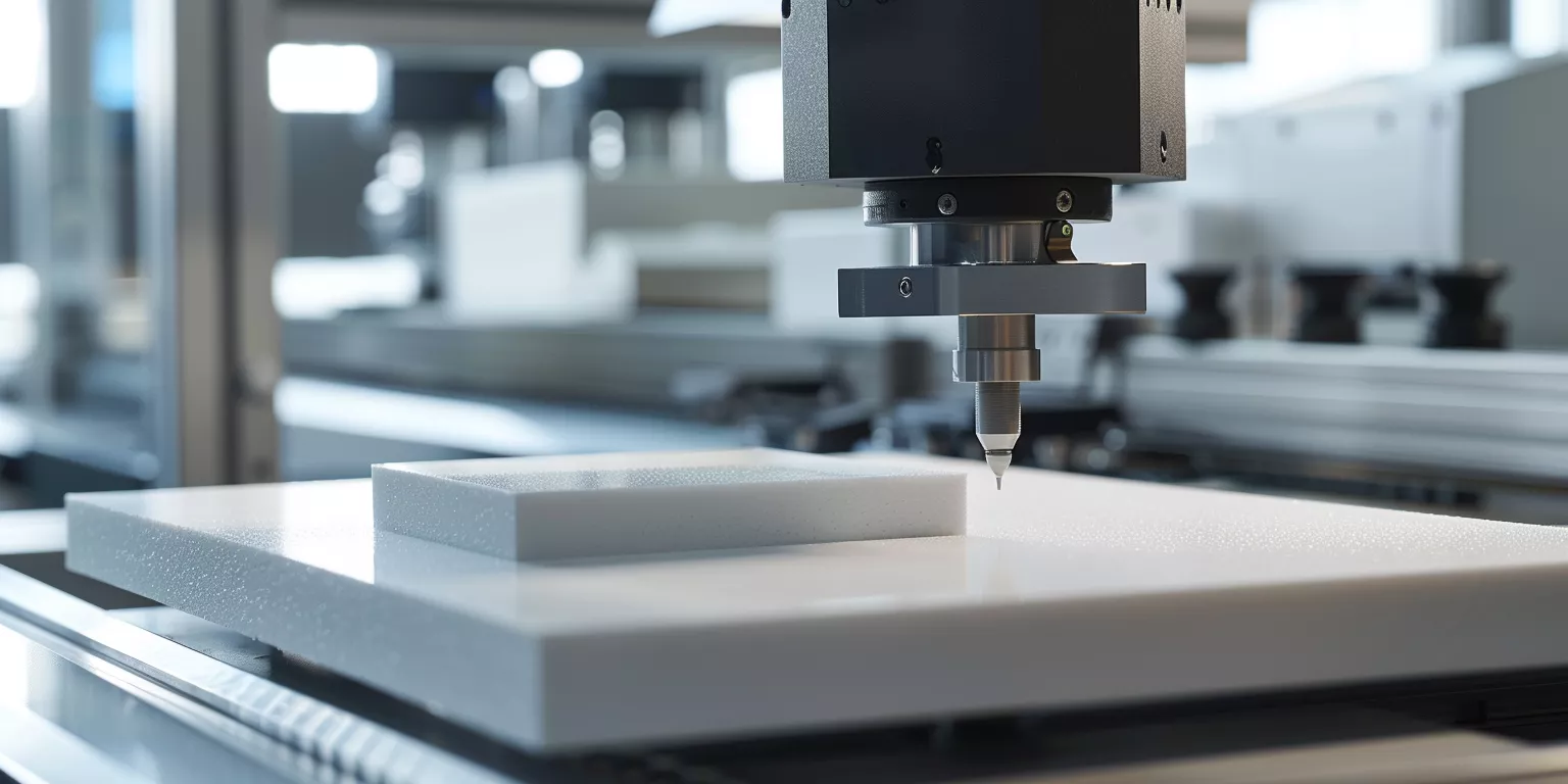
Structural bonding introduces a different performance lens for etched alumina surfaces, as mechanical load transfer and environmental durability become primary concerns. Moreover, bonding reliability depends less on visual surface condition and more on how etching modifies interfacial stress distribution2. Accordingly, etching is evaluated as a means to stabilize bonded joints3 rather than merely increase initial bond strength.
Correlation Between Surface Roughness and Bond Strength
Etched surface roughness directly influences mechanical interlocking at the bond interface. Consequently, bond strength improvements arise when surface features promote load sharing without introducing stress concentration.
In adhesive bonding trials, application-typical Ra windows near ~0.6–1.2 μm often improve shear vs polished baselines — treat shear % as illustrative / published-range screening; confirm adhesive · coupon on RFQ. Too-smooth surfaces tend toward adhesive failure; overly deep valleys can shift fracture into the ceramic. This observation confirms that optimal bonding relies on balanced roughness rather than maximum texturing.
Therefore, roughness control functions as a structural design variable rather than a secondary surface attribute.
Long-Term Stability of Bonded Interfaces on Etched Alumina
Bonded alumina assemblies are often subjected to prolonged thermal and environmental exposure. As a result, etched interfaces must retain integrity beyond initial qualification tests.
Accelerated aging examples in literature sometimes show etched joints retaining more of initial shear after hot aging than unetched stacks — treat retention % and hours as hypothetical / application-dependent; confirm aging plan on RFQ (no life SLA). Engineers evaluating field returns frequently link premature debonding to insufficient surface activation rather than adhesive formulation. These findings emphasize the role of etched microfeatures in mitigating interfacial creep and relaxation.
Accordingly, etching contributes to bond longevity by redistributing interfacial stresses under sustained loading.
Compatibility with Brazing and Coating-Based Bonding Systems
Beyond adhesives, etched alumina surfaces are also used in brazing and coating-assisted bonding systems. Consequently, surface condition affects wetting behavior and joint uniformity.
In brazed assemblies, etched alumina can improve filler wetting (softened illustrative angle reductions sometimes cited), improving flow and continuity — confirm braze system on RFQ. Coating-based bonding systems similarly benefit from etched surfaces through improved coating adhesion and reduced delamination during thermal cycling. Engineers often note that etched substrates exhibit fewer interfacial voids during post-bond inspection.
Thus, etching enhances compatibility across multiple structural bonding methodologies without altering base material composition.
Structural bonding — illustrative screening (confirm coupon RFQ)
| Parameter | Unetched (screening) | Etched (screening) |
|---|---|---|
| Application-typical Ra (μm) | ~0.1–0.3 | ~0.6–1.2 |
| Shear trend | Baseline | Illustrative published-range gains — no contract % |
| Aging retention | Often lower | Hypothetical/application-dependent — no life SLA |
| Wetting / braze flow | Limited | Softened illustrative improvement |
| Interfacial voids | More common | Often reduced when Ra matched |
| Long-term stability trend | Stackup-limited | Better when etch + adhesive/braze validated |
Process Control Parameters in Alumina Substrate Etching
Process control defines whether alumina substrate etching remains a repeatable surface-engineering step or devolves into an unpredictable risk factor. Moreover, unlike bulk ceramic processing, etching outcomes depend on tightly coupled variables that amplify small deviations. Accordingly, engineers treat parameter discipline as the primary determinant of yield and reliability rather than chemical selection alone.
Temperature Time and Concentration Interdependence
Temperature, exposure time, and chemical concentration interact nonlinearly during alumina substrate etching. Consequently, adjusting one parameter in isolation rarely produces predictable results.
In controlled baths, a modest temperature rise can accelerate etch rate (illustrative / glass-phase dependent — sometimes tens of percent per ~10 °C). Compensating only with shorter time can hurt Ra uniformity — confirm T · time · concentration coupling on DOE. Conversely, lowering concentration while extending time tends to preserve uniformity but increases sensitivity to boundary-phase dissolution. These observations confirm that stable etching relies on balanced parameter coupling rather than linear scaling.
Therefore, parameter optimization must be performed as a system-level exercise rather than through incremental adjustments.
Batch Consistency and Scale-Up Constraints
Maintaining batch-to-batch consistency becomes increasingly challenging as etching scales from laboratory samples to production lots. As a result, uniform heat distribution and chemical refresh rates dominate scale-up feasibility.
In pilot lines, batch temperature gradients (OEM-dependent; screening often cites a few °C) can drive roughness scatter that hurts metallization yield — confirm thermal uniformity on scale-up RFQ. Engineers frequently mitigate this risk by limiting batch sizes and implementing staged immersion rather than single-vessel loading. Experience shows that aggressive batch consolidation often increases scrap rates instead of reducing cost.
Accordingly, scale-up strategies prioritize thermal uniformity and controlled throughput over volumetric efficiency.
Monitoring Surface Evolution During Etching
Real-time or staged monitoring provides critical feedback during alumina substrate etching. Consequently, surface characterization becomes an integral part of process control rather than a post-process verification step.
In practice, staged Ra checkpoints during etch help catch boundary over-activation early. Facilities using checkpoints often see better run-to-run consistency (illustrative) — confirm metrology plan on RFQ. This proactive approach reduces reliance on destructive testing while preserving mechanical integrity.
Thus, monitoring transforms etching from a fixed recipe into a controlled progression aligned with material response.
Process control — OEM-/chemistry-dependent screening
| Parameter | Illustrative screening focus |
|---|---|
| Temperature stability | Hold within OEM recipe band (± few °C typical screening) |
| Exposure time | Short pilot windows; lock via DOE |
| Etch-rate variability | Expect glass-phase / grade sensitivity |
| Ra deviation | Metrology-gated; no global Ra SLA |
| Batch thermal gradient | Limit for adhesion yield |
| Yield impact if control lost | Application-dependent — confirm SPC on RFQ |
Common Engineering Failures Linked to Improper Etching
Improper etching introduces failure mechanisms that often remain hidden until late-stage testing or field operation. Consequently, these failures are frequently misattributed to metallization, bonding materials, or operating conditions rather than surface preparation errors.
-
Excessive surface roughening leading to premature fracture
Over-etching increases micro-topographical depth beyond structurally tolerant limits, particularly when valleys deepen past shallow application windows. In operational environments, such features concentrate stress and accelerate crack initiation during thermal cycling or mechanical loading. Engineers routinely encounter fracture paths that trace etched regions rather than bulk grain interiors, revealing surface preparation as the root cause. -
Non-uniform etching causing interfacial instability
Uneven temperature distribution or inconsistent exposure time produces roughness variation across a single substrate. This non-uniformity creates localized adhesion scatter (illustrative) that can promote edge lifting or partial delamination under service — confirm coupon map on RFQ. Such failures often appear sporadic, yet they originate from predictable process imbalance. -
Chemical residue retention and contamination-related defects
Inadequate post-etch cleaning leaves residual ions or reaction byproducts embedded along grain boundaries. These residues can raise leakage risk or interfere with metallization wetting — treat % deltas as illustrative; confirm post-etch clean on RFQ. Field analysis frequently links unexpected electrical drift to incomplete etchant removal rather than material defects.
Consequently, recognizing these failure patterns reinforces the need for disciplined etching control and provides a clear transition toward defining when etching should be avoided altogether in alumina substrate design.
Selecting an Etching Strategy Based on Application Demands
Selecting an appropriate etching strategy requires aligning surface modification objectives with real operating constraints rather than applying a uniform process across applications. Moreover, etching decisions influence not only surface condition but also downstream reliability, yield stability, and lifecycle cost. Accordingly, engineers evaluate etching strategies through application-driven performance priorities instead of isolated process capability.
Power Electronics and High Thermal Load Systems
Power electronic assemblies impose simultaneous electrical insulation and thermal cycling demands on alumina substrates. Consequently, etching strategies must enhance metallization adhesion without weakening structural integrity.
In these systems, controlled chemical etching toward application-typical Ra ~0.8–1.3 μm often supports stable metallization when thermal-cycle qual is matched. Deeper texturing can raise crack risk near solder joints under large ΔT — confirm module stackup on RFQ (no cycle life SLA). This experience reinforces preference for uniform chemical etching over aggressive physical methods in high thermal load environments.
Therefore, conservative surface activation remains the dominant strategy where thermal endurance defines system success.
Sensors and Precision Instrumentation
Sensors and precision instrumentation prioritize signal stability, dimensional fidelity, and surface cleanliness. As a result, etching strategies emphasize subtle surface modification rather than pronounced roughening.
In sensor housings and signal substrates, light etching within application-typical Ra ~0.4–0.8 μm often improves bonding repeatability while protecting tight tolerances. Plasma-assisted or hybrid routes can reduce contamination-related drift vs abrasive methods (illustrative) — confirm clean + metrology on RFQ. Such outcomes highlight the importance of surface chemistry control over mechanical texturing.
Accordingly, precision applications favor etching methods that preserve geometry while enhancing interface consistency.
Structural and Assembly-Oriented Applications
Structural assemblies subject alumina substrates to mechanical load transfer and environmental exposure. Consequently, etching strategies must balance anchoring strength with crack resistance.
In bonded or brazed assemblies, hybrid mild-chemical + limited physical texturing often improves shear vs polished baselines — treat % as illustrative; confirm coupon RFQ. Engineers evaluating field returns often observe that assemblies processed with overly aggressive etching exhibit early microcrack propagation under vibration. This observation underscores the need for distributed microfeatures rather than isolated deep textures.
Thus, assembly-driven designs benefit from moderate, evenly distributed surface modification strategies.
Etching strategy by application — application-typical Ra windows (not global Ra SLA)
| Application | Preferred approach | Ra / feature screening | Primary driver |
|---|---|---|---|
| Power electronics | Chemical | Ra ~0.8–1.3 | Thermal-cycle reliability (confirm qual) |
| Precision sensors | Plasma or light chemical | Ra ~0.4–0.8 | Signal stability |
| Structural assemblies | Hybrid chemical + physical | Ra ~0.6–1.2 | Load-transfer durability |
| Rework / FA | Selective chemical | Keep Ra modest | Substrate preservation |
| Microstructured interfaces | Chemical or laser-assisted | Shallow features (DOE) | Functional integration |
Lock Ra to grade · chemistry · metrology on RFQ — not a site-wide SLA.
When Etching Should Be Avoided in Alumina Substrate Design
Etching is not universally beneficial in alumina substrate design, particularly when surface modification introduces more risk than functional gain. Consequently, recognizing scenarios where etching should be deliberately excluded is as important as mastering its application.
-
Applications dominated by bulk mechanical strength requirements
In load-bearing or impact-sensitive designs, etched surface features may act as crack initiation sites under mechanical stress. Aggressively etched substrates can show flexural screening losses under vibration or shock (illustrative published-range sometimes ~10–20%) — screening only; confirm mechanical plan on RFQ. In such cases, preserving a polished or minimally processed surface provides superior structural reliability. -
High-precision dimensional tolerance constraints
Designs requiring dimensional tolerances tighter than ±0.02 mm often cannot accommodate even shallow surface recession. Minor etching-induced material loss can accumulate across multiple surfaces, complicating assembly alignment and calibration. For ultra-precision components, surface stability outweighs potential adhesion benefits. -
Electrically sensitive environments with minimal interface demands
In applications where alumina functions solely as an electrical insulator without bonded or metallized interfaces, etching offers limited value. Introducing roughness in such contexts may increase contamination retention or surface leakage risk under humidity — treat % as illustrative; skip etch when interface demand is nil. Avoiding etching in these designs reduces unnecessary processing complexity.
Accordingly, strategic restraint in applying etching ensures that alumina substrate design remains aligned with functional priorities rather than procedural convention.
RFQ Checklist for Etched Alumina Substrates
Custom etching succeeds when material behavior, surface objectives, and downstream stackup are locked before recipe trials. Use this neutral RFQ checklist — not brand CTAs — to gate metallization, bonding, microstructuring, or rework builds.
-
Application intent and stackup
State whether etch supports metallization, bonding, microstructuring, or rework. Specify industry-typical grade class (~96% / ~99% screening language or supplier 95% / 99.x% sheet), thickness, flatness, target Ra or feature depth, and metallization/adhesive system. Front-loading these fields cuts blind recipe loops. -
Process route and control window
Choose chemical, physical, or hybrid routes against the dominant constraint (uniformity vs spatial selectivity). Quote application-typical Ra windows and keep microfeatures shallow; tune for batch repeatability rather than maximum removal. Confirm chemistry · T · time · metrology on process DOE. -
Inspection, coupons, and lead time
Request drawing/tolerance review, post-etch inspection (Ra / visual / residue), and coupon peel or shear aligned to the stackup. Ask for lead time on RFQ for both standard substrates and etched lots — do not assume fixed ship SLAs. Compatibility notes for subsequent metallization or bonding belong on the same RFQ package.
For etch window · Ra · metallization RFQ support, use custom ceramic services; for grade families, see materials and alumina substrates.
Closing Perspective on Etching as a Surface Engineering Tool
Etching occupies a precise position within alumina substrate engineering, offering targeted surface modification without redefining the ceramic’s fundamental role. Accordingly, its value emerges when applied with restraint, clarity of purpose, and respect for material boundaries.
-
Etching functions as an interface enabler rather than a universal solution
Etching improves interaction at interfaces where adhesion, bonding, or functional integration is required, yet it does not enhance bulk alumina properties such as stiffness or fracture toughness. Engineers consistently find that surface modification delivers the greatest benefit when paired with clearly defined downstream requirements. This perspective prevents etching from being misapplied as a corrective measure for unrelated design limitations. -
Material-aware application determines long-term reliability
Successful etching strategies account for alumina’s grain structure, purity, and brittleness before any process parameters are selected. Ignoring these constraints often leads to hidden reliability risks that surface only during extended operation. Material-aware application ensures that surface gains do not translate into structural compromises. -
Process discipline outweighs procedural complexity
Reliable outcomes depend more on disciplined control of exposure, temperature, and uniformity than on sophisticated equipment or aggressive chemistries. In production environments, simpler and well-controlled etching routes frequently outperform complex, loosely managed alternatives. Consistency, rather than intensity, defines sustainable surface engineering practice.
Consequently, etching remains most effective when treated as a deliberate surface engineering tool, applied only where it meaningfully supports functional performance and system reliability.
Conclusion
Alumina Substrate Etching enables controlled surface functionality when material behavior, process limits, and application demands are aligned with engineering intent rather than routine practice.
If your application requires controlled alumina substrate etching for metallization, bonding, microstructuring, or rework, package grade class, target Ra, stackup, coupon peel/shear plan, and lead time on RFQ before locking production recipes. Start from custom ceramic services or browse materials and alumina substrates.
Related reading
- Alumina substrate thickness: dielectric, thermal & RFQ windows — when the limiter is alumina substrate thickness (mm dielectric/thermal window), not etch chemistry or Ra targets.
- How to clean Al₂O₃ substrate without residue or surface damage — when the bottleneck is pre/post-etch cleaning without residue or surface damage, not etch recipe selection.
- Alumina substrate vs FR4 for high-power electronics — when the decision is alumina substrate vs FR4 board material, not whether/how to etch alumina.
FAQ
What surface roughness range is typically recommended for Alumina Substrate Etching?
Application-typical screening often cites Ra ~0.6–1.5 μm as a starting band for adhesion vs structural safety — not a global Ra SLA. Values outside this band need grade · chemistry · metrology justification and coupon testing on RFQ.
Can Alumina Substrate Etching affect electrical insulation performance?
When properly controlled, etching does not degrade electrical insulation. However, excessive roughness or residual contamination may increase surface leakage risk under high humidity.
Is Alumina Substrate Etching suitable for high-purity substrates?
Yes, but higher-purity / ~99% industry-typical classes exhibit slower etch kinetics and narrower windows than ~96% class substrates (screening language; align to supplier grade sheets). Parameter control is more critical — confirm on process DOE.
Can etched alumina substrates be reliably re-metallized after rework?
Selective etching with limited exposure time often allows re-metallization when post-etch cleaning is thorough and Ra stays within the application-typical rework limit for the next stackup — confirm on coupon RFQ.
References:
-
Explore this link to understand how Mo-Mn metallization enhances thermal compatibility and reliability in electronic applications. ↩
-
Understanding this concept is crucial for improving bonding techniques and ensuring long-lasting structural integrity. ↩
-
See how etching techniques relate to bonded-joint stability and durability in structural assemblies. ↩