Semiconductor Ceramics in Industrial Process Systems
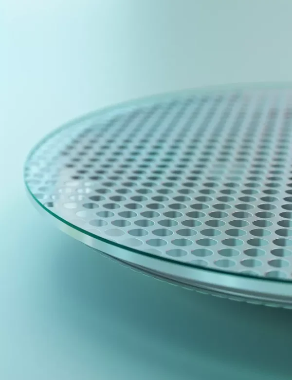
Semiconductor ceramics are precision ceramic components used in semiconductor manufacturing equipment. They provide electrical insulation, thermal management, dimensional stability, and support for plasma, vacuum, and chemical environments.
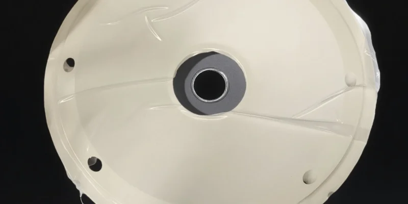
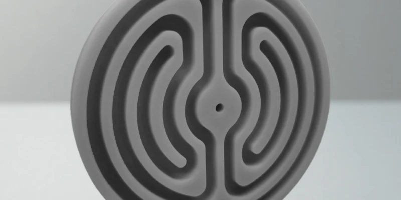
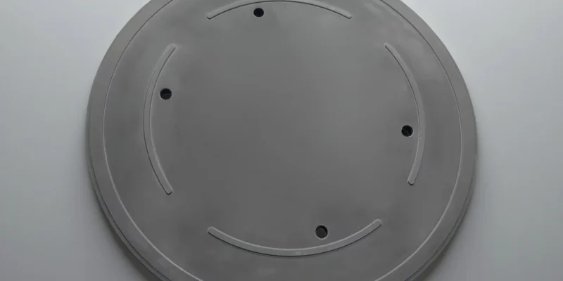
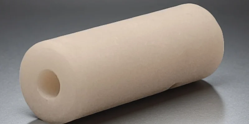
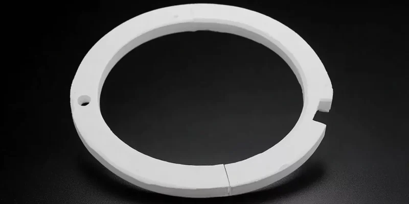
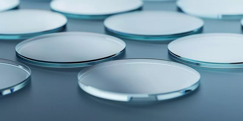
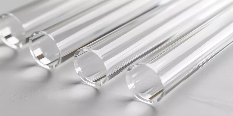
Typical parts include chamber liners, focus rings, insulators, heaters, chucks, end effectors, lift pins, carriers, windows, and tubes used in etching, deposition, thermal processing, and wafer handling.
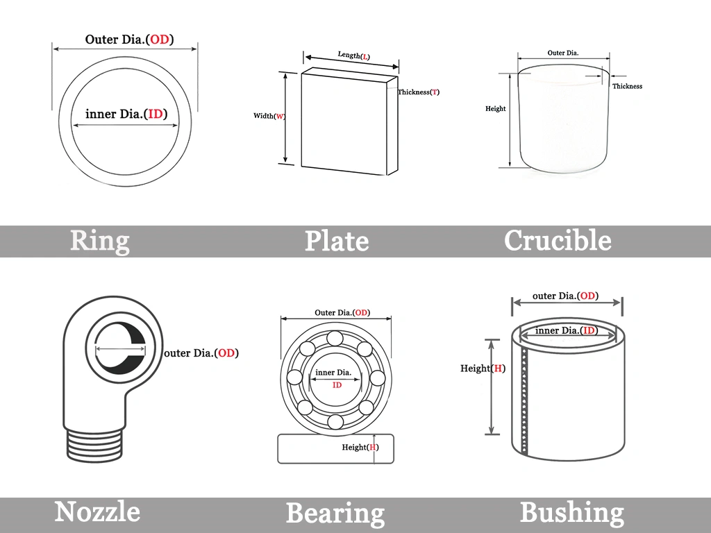
ADCERAX manufactures custom components from drawings, samples, or old-part references. We review the material, dimensions, tolerances, surfaces, and operating conditions before confirming manufacturability.
withstands sustained high temperature cycling
resists plasma and corrosive gases
maintains resistance under elevated voltage
preserves geometry under mechanical stress
ADCERAX Material Properties of Semiconductor Ceramics
In semiconductor manufacturing, material choices are evaluated through quantifiable thermal, electrical, chemical, and mechanical behavior rather than nominal grades, allowing semiconductor ceramics to be compared and selected against real process constraints.
Thermal Properties
| Ceramic Material | Max Continuous Service Temp (°C) | Thermal Conductivity (W/m·K) | CTE (×10⁻⁶/K, 20–800 °C) | Test Conditions |
|---|---|---|---|---|
| Alumina (Al₂O₃, 99.7%) | 1650 | 25–30 | 7.8 | Air, steady-state |
| ZTA | 1500 | 18–22 | 8.0 | Air, steady-state |
| Zirconia (Y-TZP) | 1000 | 2.5–3.0 | 10.5 | Air, steady-state |
| Silicon Carbide (SSiC) | 1600 | 120–180 | 4.2 | Inert atmosphere |
| Boron Nitride (HPBN) | 1800 | 30–60 | 1.0 | Inert atmosphere |
| Silicon Nitride (Si₃N₄) | 1400 | 25–35 | 3.2 | Air, steady-state |
| Aluminum Nitride (AlN) | 1400 | 170–200 | 4.5 | Air, steady-state |
| Boron Carbide (B₄C) | 1500 | 30–42 | 5.6 | Air, steady-state |
| Metallic Ceramics (Cermet) | 1000 | 20–50 | 6.0 | Air, steady-state |
| Sapphire (Al₂O₃ single crystal) | 1700 | 35 | 5.6 | Air, steady-state |
| Beryllium Oxide (BeO) | 1600 | 250–330 | 7.5 | Air, steady-state |
| Yttria (Y₂O₃) | 1700 | 12–15 | 8.1 | Plasma-compatible |
Electrical Properties of Semiconductor Ceramics
| Ceramic Material | Volume Resistivity (Ω·cm) | Dielectric Strength (kV/mm) | Dielectric Constant (1 MHz) | Test Conditions |
|---|---|---|---|---|
| Alumina (99.7%) | ≥10¹⁴ | 12–15 | 9.6 | 25 °C, dry |
| ZTA | ≥10¹³ | 10–12 | 10.0 | 25 °C, dry |
| Zirconia | ≥10¹² | 8–10 | 29 | 25 °C, dry |
| Silicon Carbide (SSiC) | 10⁵–10⁶ | 2–4 | 9.7 | 25 °C |
| Boron Nitride (HPBN) | ≥10¹⁵ | 3–4 | 4.0 | 25 °C |
| Silicon Nitride | ≥10¹⁴ | 12–14 | 7.8 | 25 °C |
| Aluminum Nitride | ≥10¹³ | 15–17 | 8.9 | 25 °C |
| Boron Carbide | 10²–10³ | 1–2 | 10.2 | 25 °C |
| Metallic Ceramics | 10⁶–10⁹ | 3–6 | 12–18 | 25 °C |
| Sapphire | ≥10¹⁵ | 15–18 | 9.4 | 25 °C |
| Beryllium Oxide | ≥10¹⁴ | 10–12 | 6.7 | 25 °C |
| Yttria | ≥10¹⁴ | 8–10 | 14–16 | 25 °C |
Chemical Stability of Semiconductor Ceramics
| Ceramic Material | Plasma Resistance | Acid Resistance (HF/HCl) | Alkali Resistance | Test Conditions |
|---|---|---|---|---|
| Alumina | Medium | Limited / Good | Good | ICP plasma, 200 h |
| ZTA | Medium | Limited / Good | Good | ICP plasma, 200 h |
| Zirconia | Medium | Moderate / Good | Moderate | ICP plasma, 200 h |
| Silicon Carbide | High | Excellent / Excellent | Excellent | ICP plasma, 300 h |
| Boron Nitride | Medium | Excellent / Excellent | Good | Inert gas |
| Silicon Nitride | High | Good / Excellent | Good | ICP plasma |
| Aluminum Nitride | Medium | Limited / Good | Moderate | Dry plasma |
| Boron Carbide | High | Excellent / Excellent | Excellent | ICP plasma |
| Metallic Ceramics | Medium | Moderate / Moderate | Moderate | Process gas |
| Sapphire | Medium | Good / Excellent | Good | Wet chemical |
| Beryllium Oxide | Medium | Good / Good | Moderate | Wet chemical |
| Yttria | Very High | Excellent / Excellent | Excellent | Plasma etch |
Mechanical Properties of Semiconductor Ceramics
| Ceramic Material | Flexural Strength (MPa) | Hardness (HV) | Fracture Toughness (MPa·m¹ᐟ²) | Test Conditions |
|---|---|---|---|---|
| Alumina (99.7%) | 320–380 | 1400–1600 | 3.5–4.0 | 4-point bend |
| ZTA | 450–650 | 1300–1500 | 6.0–7.0 | 4-point bend |
| Zirconia | 900–1200 | 1200–1300 | 7.0–10.0 | 4-point bend |
| Silicon Carbide | 400–450 | 2400–2800 | 3.5–4.5 | 4-point bend |
| Boron Nitride | 70–100 | 300–400 | 2.0–2.5 | 3-point bend |
| Silicon Nitride | 700–900 | 1500–1700 | 6.0–7.5 | 4-point bend |
| Aluminum Nitride | 300–350 | 1100–1200 | 2.5–3.0 | 4-point bend |
| Boron Carbide | 350–400 | 3000–3800 | 2.5–3.5 | 4-point bend |
| Metallic Ceramics | 500–800 | 900–1300 | 5.0–8.0 | 4-point bend |
| Sapphire | 400–500 | 2000 | 3.0–4.0 | 4-point bend |
| Beryllium Oxide | 300–350 | 1100 | 2.5–3.0 | 4-point bend |
| Yttria | 180–250 | 600–800 | 2.0–2.5 | 4-point bend |
Ceramic Functional Applications Across Semiconductor Manufacturing
Below, ADCERAX groups semiconductor ceramics by real process functions rather than by material names, reflecting how engineers and buyers evaluate ceramics for semiconductor equipment in actual production lines.
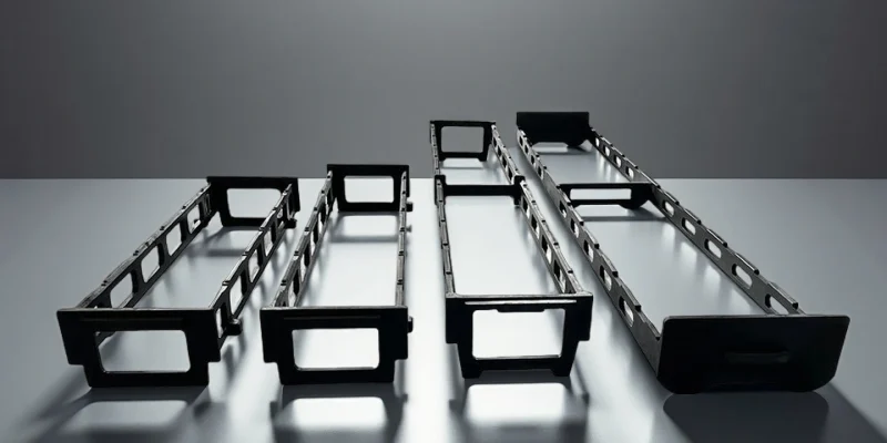
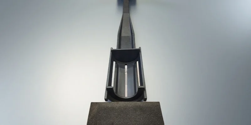
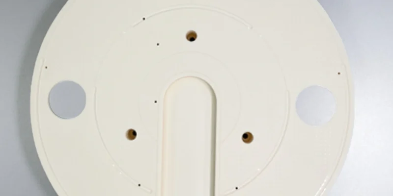
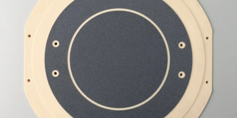
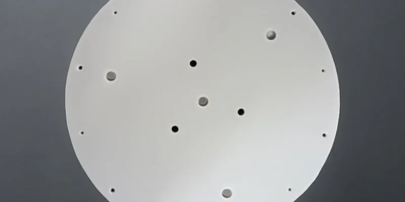
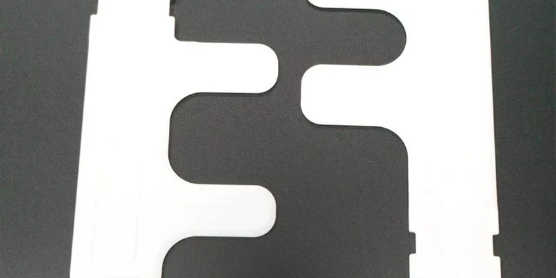
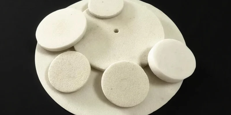
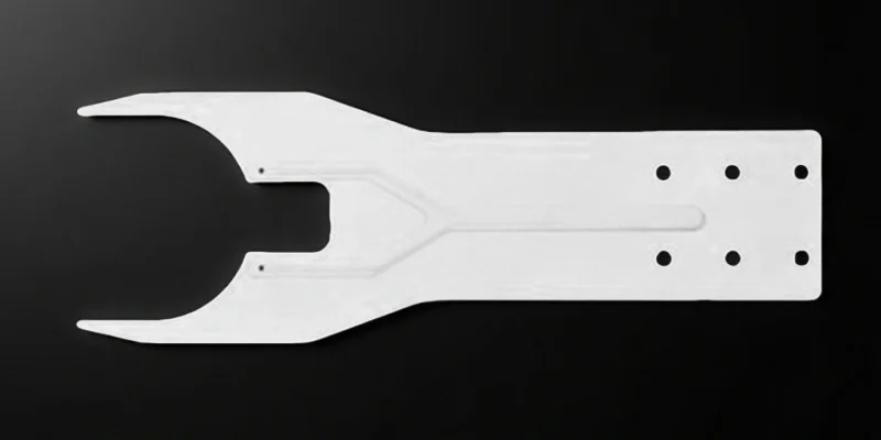
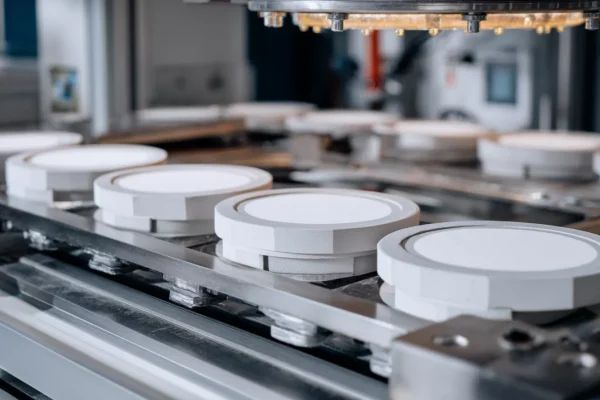
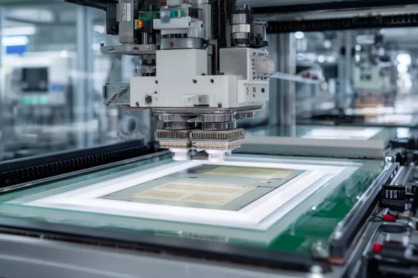
Wafer Handling and Positioning
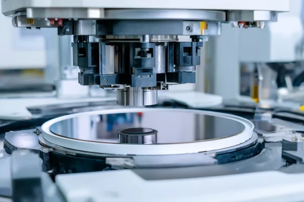
Semiconductor manufacturing relies on controlled wafer fixation and movement, where ceramic interfaces directly affect yield stability and contamination control.
- Dimensional stability supports repeatable wafer alignment during processing.
- Low particle generation reduces defect risks in high-value wafers.
- Thermal compatibility maintains accuracy across temperature transitions.
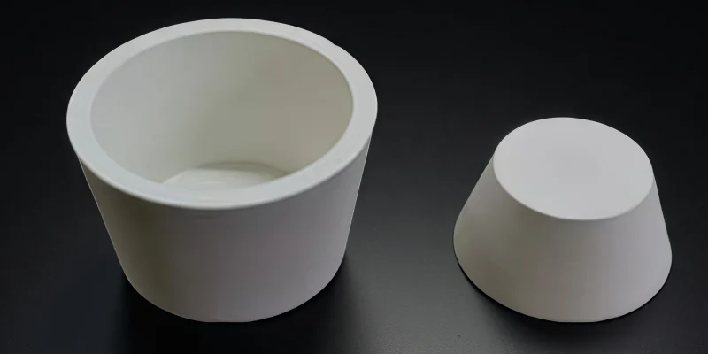
Thermal Processing and Furnace Systems
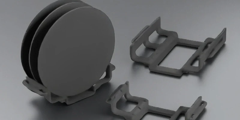
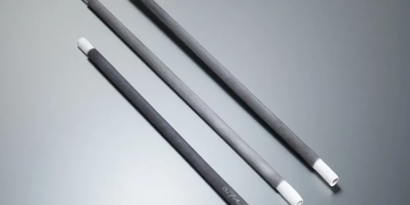
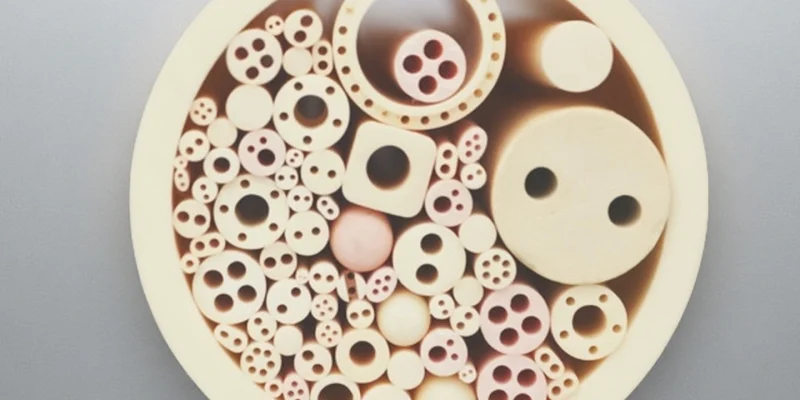
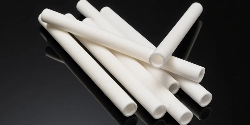
High-temperature process steps rely on ceramic components that remain chemically inert and dimensionally stable throughout extended furnace cycles.
- Thermal shock resistance enables repeated heating and cooling without structural failure.
- Chemical inertness limits ionic release and surface reactions at elevated temperatures.
- Creep stability preserves geometry during long-duration thermal exposure.

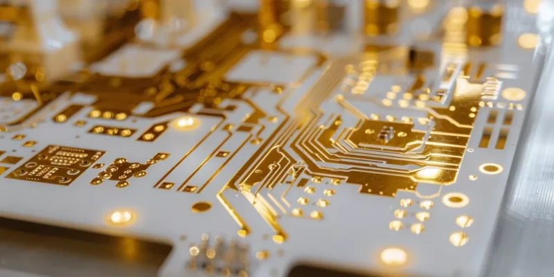
Substrates and Electrical Packaging
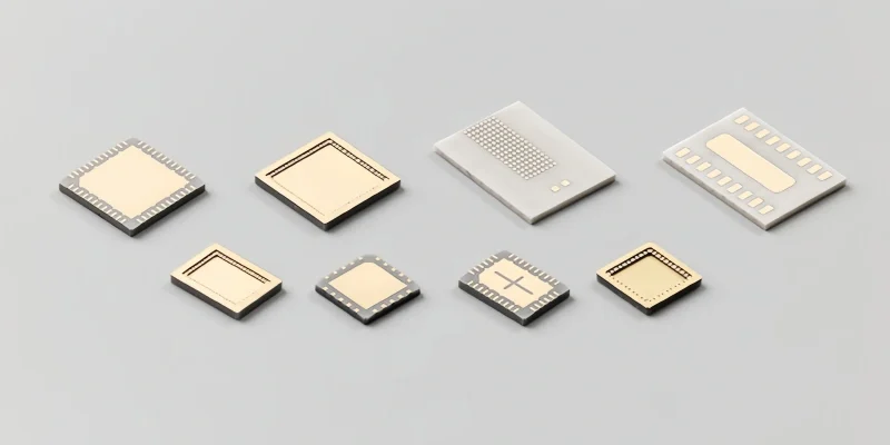
Electrical isolation and heat dissipation converge in ceramic substrates used for power devices and advanced packaging.
- Electrical insulation ensures stable signal separation at high voltages.
- Thermal conductivity supports efficient heat dissipation paths.
- Metallization compatibility enables reliable circuit integration.
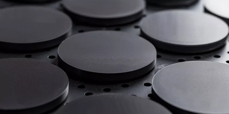
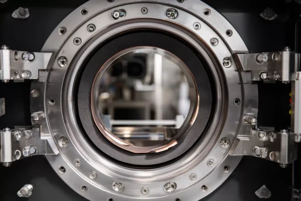
Plasma Etching and Coating Chambers
Plasma-facing zones rely on ceramics that hold surface integrity under ion bombardment, reactive radicals, and long vacuum exposure.
- Plasma resistance reduces erosion and particle generation at the surface.
- Chemical stability withstands corrosive etch byproducts during chamber cycles.
- Electrical insulation supports repeatable bias control and uniform discharge.
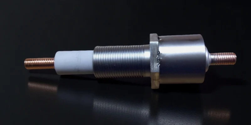
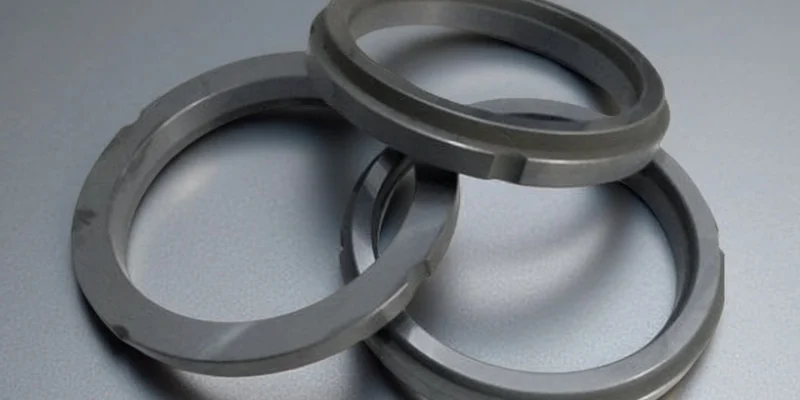
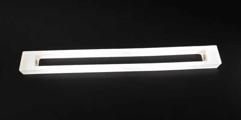
Precision Tools and Wear Components
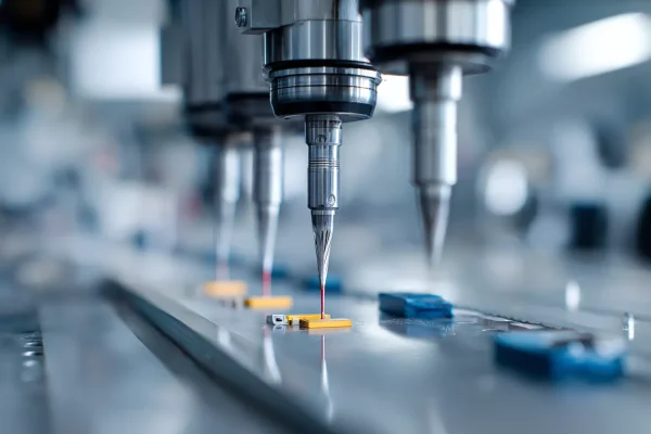
Localized contact, cutting, and bonding operations depend on ceramics with controlled wear and geometric accuracy.
- Wear resistance extends service life in repetitive motion.
- Edge integrity maintains consistent cutting and bonding quality.
- Mechanical strength supports micron-level precision operations.
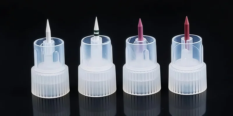
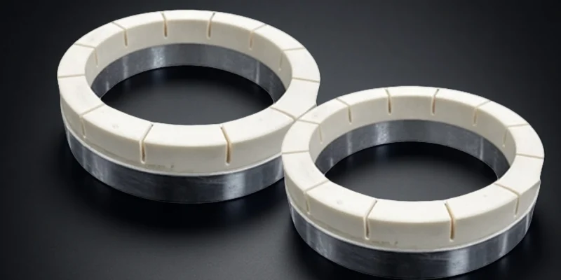
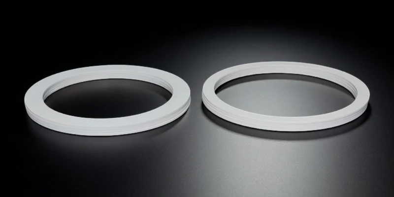
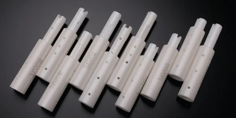
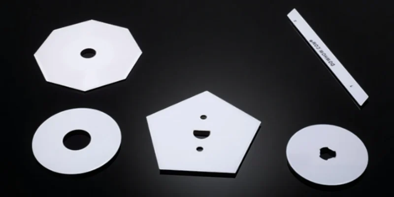
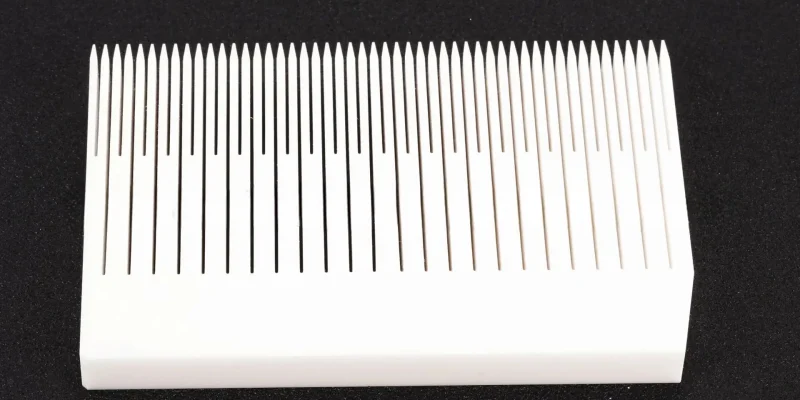
From Application Needs to Ceramic Solutions
Each semiconductor process zone places distinct demands on ceramic performance and geometry control.
ADCERAX translates application conditions into manufacturable ceramic solutions.
ADCERAX Semiconductor Ceramics Portfolio Structure
This classification reflects how semiconductor ceramics are selected, qualified, and deployed across process tools rather than how they are manufactured.

Alumina Ceramic
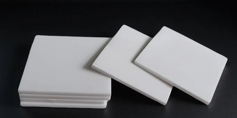
Alumina ceramics remain the most widely used semiconductor process ceramic parts due to balanced purity, insulation, and cost control.

Zirconia Ceramic
Zirconia ceramics are selected for technical ceramics semiconductor applications requiring precision and wear stability.
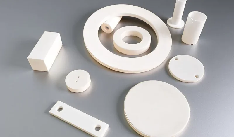
ZTA Ceramics
Zirconia Toughened Alumina combines alumina stability with enhanced fracture resistance for mechanically stressed zones.
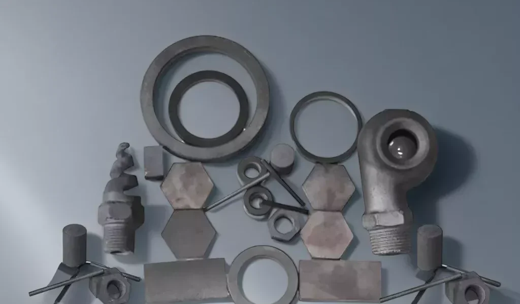
Silicon Carbide Ceramics
Silicon carbide ceramic parts are selectively used for electrically adjacent high-temperature or wear-intensive applications.
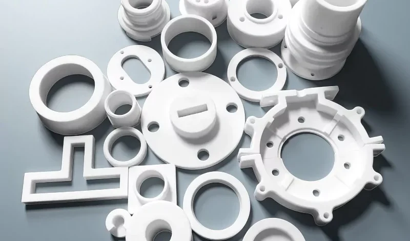
Boron Nitride Ceramics
Boron nitride electrical ceramics provide insulation performance under high temperature with non-wetting characteristics.
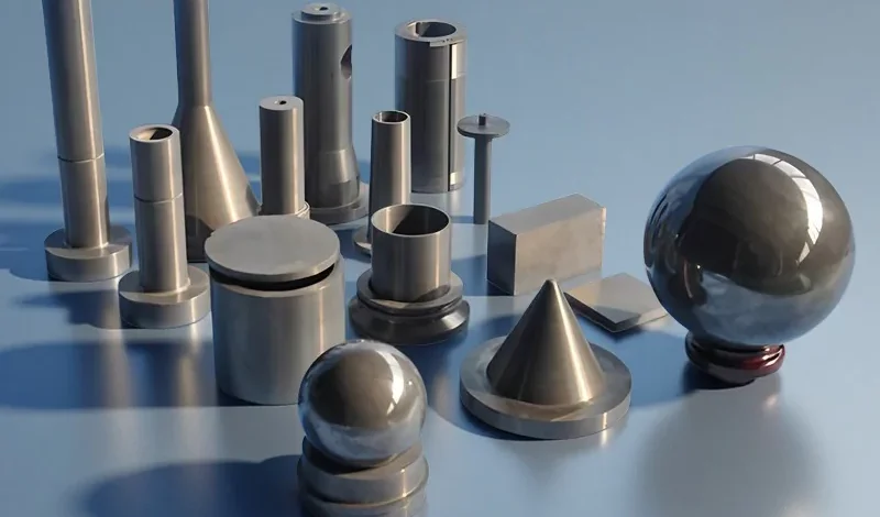
Silicon Nitride Ceramics
Silicon nitride electrical ceramic parts combine structural reliability with thermal endurance in electrically stressed environments.
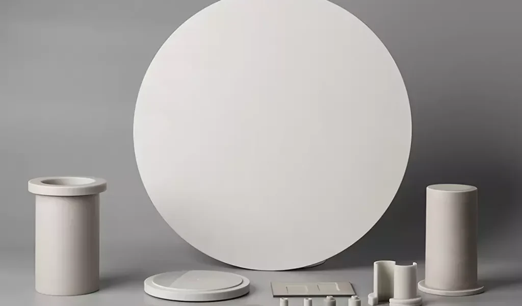
Aluminum Nitride Ceramics
Aluminum nitride ceramics support metallurgical systems requiring efficient heat dissipation with electrical insulation.
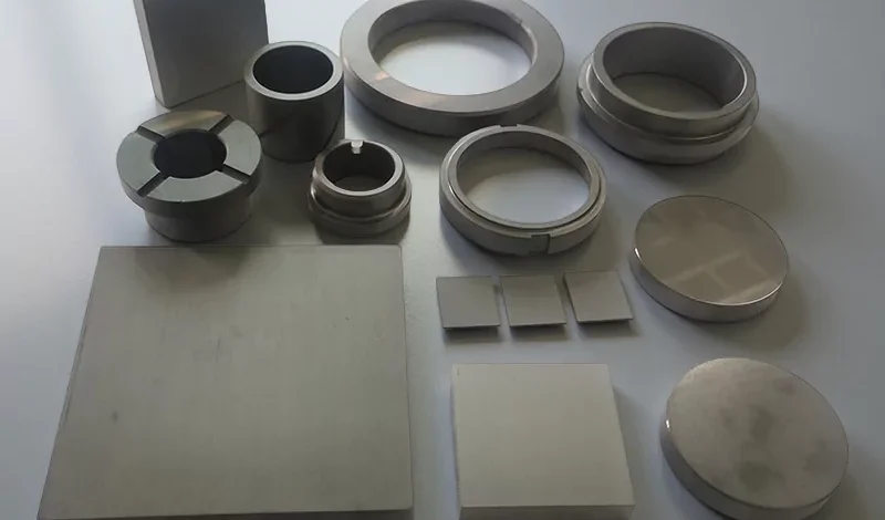
Boron Carbide Ceramics
Boron carbide ceramics serve extreme wear zones where hardness dominates material selection.
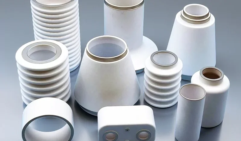
Metallized Ceramics
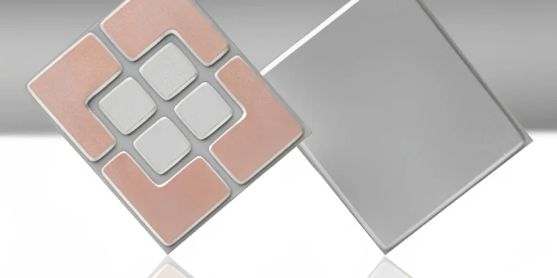
Metallized electrical ceramic components integrate conductive interfaces for electrical connection and packaging.
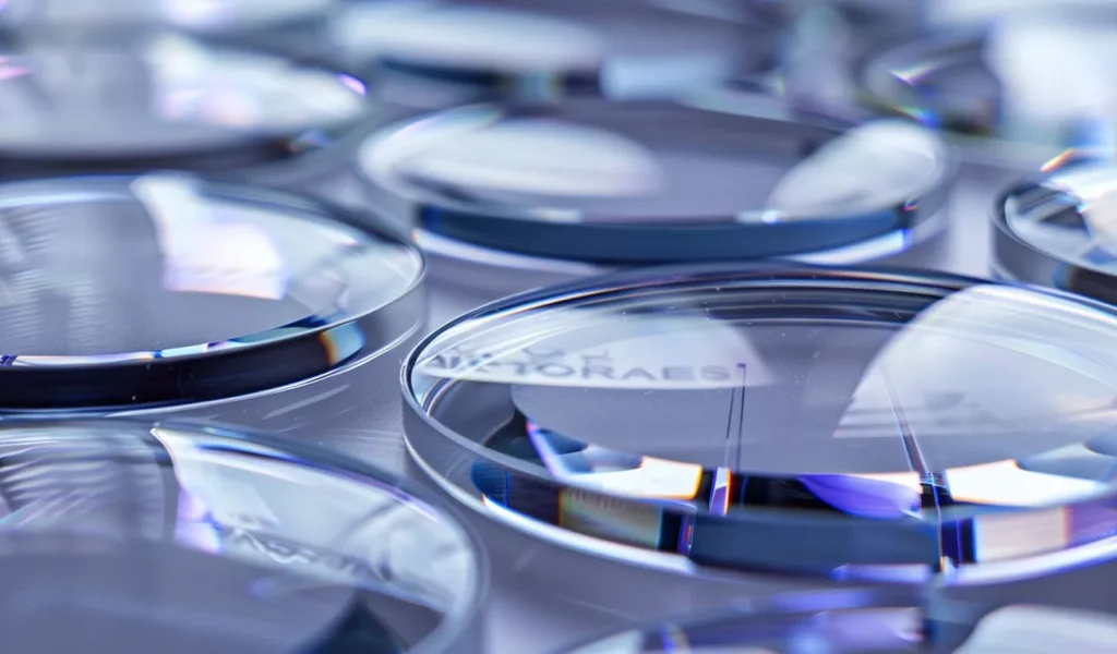
Transparent Ceramics
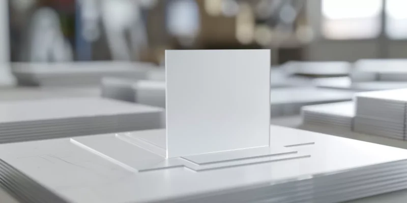
Transparent ceramics support optical and inspection-related technical ceramics semiconductor applications.
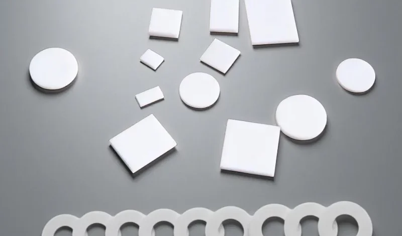
BeO Ceramics
Beryllium oxide ceramics are applied where high purity ceramic parts for semiconductor require maximum heat dissipation.
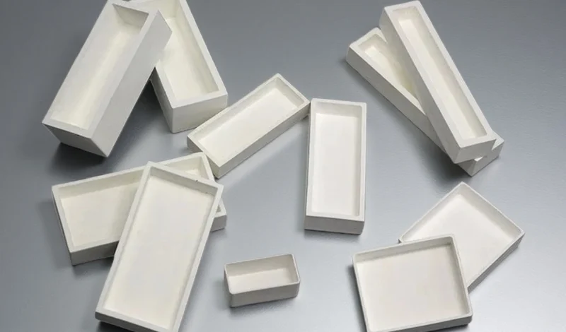
Yttria Ceramics
Yttria ceramics are widely used in plasma-facing semiconductor ceramics.
Integrated Manufacturing Support for Semiconductor Ceramics
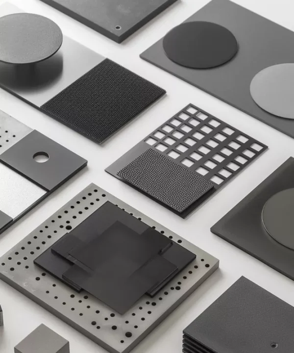
ADCERAX provides coordinated manufacturing workflows for semiconductor ceramics, covering material preparation, precision forming, finishing, and verification within a single supply chain.
Each process stage is aligned with equipment requirements to support reliable delivery of ceramics for semiconductor equipment without fragmented sourcing.
match ceramic grades to process environments
press, cast, or extrude complex ceramic geometries
achieve tight tolerances on functional ceramic parts
control roughness and edge integrity consistently
apply DBC DPC or HTCC conductive layers
verify interfaces with metal or composite components
ADCERAX Machining Capabilities for Semiconductor Ceramics
Precision Ceramic Sintering Control
Controlled sintering defines final density, grain structure, and dimensional stability for semiconductor ceramics used in thermal and plasma processes.
stable firing up to 1700 °C ±5 °C
oxygen nitrogen vacuum selectable per material
≥99.5% theoretical density across batches
Accurate CNC Ceramic Machining
Post-sinter machining enables custom semiconductor ceramic parts to meet strict assembly and alignment requirements.
complex geometries without stress concentration
dimensional accuracy down to ±0.01 mm
Ra ≤0.4 µm on functional interfaces
Metallization & Interface Processing
Metallized ceramics support electrical and thermal integration in ceramics for semiconductor equipment, especially packaging and power modules.
copper thickness 0.2–0.8 mm selectable
peel strength ≥6 N/mm verified
flatness ≤0.15% after metallization
Custom Semiconductor Ceramics Built Around Your Process
ADCERAX supports custom semiconductor ceramic development by translating application conditions, drawings, and tolerance requirements into manufacturable ceramic solutions.
From geometry optimization to material selection, each customization step focuses on fit, consistency, and integration with semiconductor equipment environments.
Start a technical discussion with ADCERAX to align your ceramic design with real process conditions.
FAQs About ADCERAX Semiconductor Ceramics
Semiconductor Ceramics are selected primarily for low outgassing, chemical inertness, and stable surface chemistry under vacuum and plasma exposure.
These properties prevent ionic release and particle generation that could directly impact wafer yield.
ADCERAX controls raw material purity and sintering density to ensure Semiconductor Ceramics remain stable throughout long process cycles.
This stability prevents creep, warpage, and alignment drift during diffusion, oxidation, and annealing steps.
ADCERAX Semiconductor Ceramics are engineered to sustain repeated thermal cycling without structural degradation.
This resistance minimizes particle shedding that could otherwise cause defect formation on wafers.
ADCERAX applies material selection and surface finishing strategies specifically for plasma-exposed ceramic components.
Semiconductor Ceramics combine high stiffness with low thermal expansion, ensuring precise wafer positioning.
These characteristics prevent deformation during temperature changes and mechanical loading.
ADCERAX supplies Semiconductor Ceramics that support repeatable wafer handling without inducing stress or misalignment.
High dielectric strength and volume resistivity allow Semiconductor Ceramics to isolate electrical fields reliably.
This insulation stability is essential in electrostatic chucks, heaters, and chamber assemblies.
ADCERAX verifies electrical performance to ensure Semiconductor Ceramics remain insulating under elevated temperature and voltage.
In applications such as heater plates and substrates, efficient heat transfer is critical for temperature uniformity.
Materials like aluminum nitride ceramics balance insulation with high thermal conductivity.
ADCERAX selects Semiconductor Ceramics that manage heat flow without sacrificing electrical isolation.
Surface roughness directly influences particle adhesion and cleaning efficiency.
A controlled finish minimizes contamination risks in wafer-facing applications.
ADCERAX manages surface finishing to meet functional requirements for Semiconductor Ceramics.
Ceramic substrates provide electrical insulation, thermal management, and mechanical support simultaneously.
This multifunctional performance enables reliable power and signal integration.
ADCERAX® develops Semiconductor Ceramics aligned with DBC, DPC, and HTCC packaging needs.
High-purity Semiconductor Ceramics reduce this risk by maintaining chemical stability.
ADCERAX® controls raw materials and processing to meet purity expectations.
Stable ceramic components reduce unexpected failures caused by thermal shock or chemical attack.
This reliability lowers maintenance interventions and unplanned stoppages.
ADCERAX Semiconductor Ceramics are designed for predictable performance across production cycles.
It depends on the equipment position and duty. Alumina suits insulators, domes and general chamber parts; aluminum nitride for heaters, ESCs and stages needing heat spreading with insulation; silicon carbide (including CVD SiC) for plasma-facing parts and low-particle wafer tables; quartz or sapphire for windows and optical/high-temperature parts. The figures we show are typical route-screening values (industry references), not certified semiconductor-grade data — we confirm the route against your drawing and process.
We work as a custom and backup manufacturer from your drawing, sample and process conditions. We don't claim semiconductor grade, cleanroom packaging or a certification unless the documentation exists for your specific part; purity, surface, traceability and packaging requirements are agreed at engineering and procurement review rather than promised up front.
Plasma-facing parts commonly use silicon carbide (including CVD SiC) or high-purity alumina, chosen for plasma resistance and low particle generation. The right choice depends on the etch chemistry, cleanliness target and geometry, which we review from your part — we don't promise a fixed life or a drop-in match to a specific tool.
Discuss Your Semiconductor Ceramic Requirements
To review your semiconductor ceramic component, please share:
- The equipment and process position (etch, deposition, wafer handling, chuck/stage, chamber)
- The part name and function; a drawing, sample or photo
- The material, purity and surface requirement if known (alumina, AlN, SiC, quartz or sapphire); dimensions and tolerance
- The process conditions (plasma, vacuum, temperature, chemistry)
- The quantity or annual demand.
ADCERAX will review material selection, geometry, manufacturing feasibility, and inspection needs. If no drawing is available, send photos, key dimensions, and operating conditions.
*Our team will answer your inquiries within 24 hours.
*Your information will be kept strictly confidential.
info@adcerax.com
Tel:+86-0731-84428843
WhatsApp:+86 19311583352
Within 24 hours